Download
1 / 10
100 likes | 436 Views
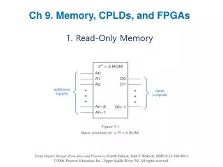
Chapter 10. Memory, CPLDs, and FPGAs. 10.1 Read-Only Memory. A read-only memory (ROM) is a combinational circuit with n inputs and b outputs. (Fig. 10-1) A ROM stores the truth table of an n-input, b-output combinational logic function. A decoder implemented by ROM (Table 10-1, Fig. 10-2)

E N D
10.1 Read-Only Memory • A read-only memory (ROM) is a combinational circuit with n inputs and b outputs. (Fig. 10-1) • A ROM stores the truth table of an n-input, b-output combinational logic function. • A decoder implemented by ROM (Table 10-1, Fig. 10-2) • ROM is a kind of non-volatile memory. • A 4x4 multiplier implemented by ROM. (Table 10-3) • Internal structure of A diode ROM. (Fig. 10-5) • A ROM using two-dimensional decoding. (Fig. 10-7) • Internal structure of a MOS transistor ROM (Fig. 10-8)
Commercial ROM types (Table 10-5) • Mask ROM • Programmable Read-Only Memory (PROM) • Erasable Programmable Read-Only Memory (EPROM) • Floating gate technology (Fig. 10-10) • Programmed by applying a HIGH voltage on the non-floating gate, and erased by exposing it to ultra-violet light. • Electrically Erasable Programmable Read-Only Memory (EEPROM) • Flash ROM • Some standard ROMs (Fig. 10-11) • Output Enable (OE) to control tri-state outputs. • Chip-Select (CS) to enable the ROM chip. • Address decoding of ROM applications (Fig. 10-12)
ROM for low power application (Fig. 10-13) • ROM timing (Fig. 10-14) • tAA: Access time from address. • tACS: Access time from chip select. • tOE: Output Enable time. The propagation delay from OE and CS both asserted until the output drivers have left the Hi-Z state. • tOZ: Output-Disable Time • tOH: Output-Hold time
10.2 Read/Write Memory • RAM (Random Access Memory): most popular read/write memory. The time it takes to read/write a bit of memory is independent of the bit’s location. • Static RAM (SRAM) • Dynamic RAM (DRAM) • SRAM and DRAM are both volatile. • Ferroelectric RAM • A kind of non-volatile RAMs.
10.3 Static RAM • Basic structure of an SRAM (Fig. 10-19) • Read operation • Write operation • Internal structure of an SRAM • RAM cell (Fig. 10-20) • A 8x4 SRAM • SRAM timing • Read timing (Fig. 10-22) • tAA: Access time from address • tACS: Access time from chip select • tOE: Output-Enable time • tOZ: Output-Disable time • tOH: Output-Hold time
Write timing (Fig. 10-23) • tAS: Address setup time before write • tAH: Address hold time after write • tCSW: Chip-select setup before end of write • tWP: Write pulse width • tDS: Data setup time before end of write • tDH: Data hold time after end of write • WE-controlled write versus CS-controlled write (Fig. 10-23) • Standard static RAMs (Fig. 10-24) • Asynchronous SRAM and Synchronous SRAM
10.4 Dynamic RAM • DRAM structure and operation • A DRAM cell (Fig. 10-31) • Write operation • Setting the word line to 1. • To store a 1, a HIGH voltage is placed on the bit line, which charges the capacitor through the “on” transistor. • To store a 0, a LOW voltage is placed on the bit line, which discharges the capacitor through the “on” transistor. • Read operation • The bit line is first precharged to a voltage halfway between HIGH and LOW. • The word line is set HIGH so that the precharged bit line is pulled slightly higher or slightly lower. • A sense amplifier detects this small change and recovers a 1 or 0 accordingly.
Reading a DRAM cell destroy the original voltage stored on the capacitor, the DRAM cell must be written back the original data after reading. • DRAM refresh (Fig. 10-32) • Internal structure of a 64Kx1 DRAM (Fig. 10-33) • Multiplexed address inputs • RAS_L: Row address strobe to store the higher order bits of the address into the row-address register. • CAS_L: Column address strobe to store the lower order bits of the address into the column-address register. • Row latches: the latches used to store data input/output from the memory array. • DRAM timing • RAS-only refresh-cycle timing (Fig. 10-34) • Read cycle (Fig. 10-35) • Write cycle (Fig. 10-36) • Synchronous DRAM
10.5 Complex Programmable Logic Devices • 10.6 Field-Programmable Gate Arrays (FPGA) • Xilinx XC4000 FPGA family • Configurable logic block (CLB) (Fig. 10-44) • Configurable interconnect structure (Fig. 10-46) • CLB and wiring details (Fig. 10-47)