Download
1 / 20
200 likes | 319 Views
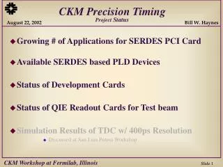
Simulation Only. Common Design for Multiple Timing Applications Available PLD Based SERDES Devices Time to Digital Converter (TDC) w/ PLD Based SERDES Timing Distribution System (TDS) w/ PLD Based SERDES Other PLD Based SERDES Potential Applications

E N D
Simulation Only • Common Design for Multiple Timing Applications • Available PLD Based SERDES Devices • Time to Digital Converter (TDC) w/ PLD Based SERDES • Timing Distribution System (TDS) w/ PLD Based SERDES • Other PLD Based SERDES Potential Applications • Simulation Results of TDC w/ 400ps Resolution • Prototype TDC/TDS Card Status
Available PLD Based SERDES Devices • Cypress Programmable Serial Interface (PSI) • CPLD w/ a single channel 2.5Gbs SERDES device • Cost ~ $140 • CPLD w/ a quad channel 1.5Gbs SERDES device • Cost ~ $200 • Both devices in production • Xilinx-II Pro FPGA • Up to 16-channel FPGA w/ 3.125 Gbs SERDES devices • Not in production & Cost is UNK • AlteraStratix FPGA • Up to 80-channel FPGA w/ 800 Mbs SERDES devices • Not in production & Cost is UNK
High-Resolution TDC Block Diagram General I/O 156 MHz Ref Clk 16bit Data Serial Receiver (Cypress / Xilinx) Detector Output (CML) FPGA/CPLD ( Cypress / Xilinx ) General I/O Serdes Control General I/O
Programmable TDC Features • Resolution of 400ps (or better) is possible • Single channel Cypress PSI w/ 2.5 Gbs SERDES (in production) • Multiple channel FPGAs planned by several vendors • Single & Multiple channel dedicated SERDES • Available or Planned by several vendors • 8 channel TDC at lower resolution (666 ps) • 4-channel Cypress device (in production) • 8-channel Cypress device (planned) • 80 channels at lower resolution (1.25 ns) • Altera Stratix FPGA • Not in production • Fully Programmable (VHDL) Backend • Timing compensation • Interface to external world (PCI, CPCI, etc.) • Transmit TDC data over one of the serial links
TDC w/ 400ps Resolution • Input Pulse Width = FFFF F800 0000-> 21bits x 6.4ns/16 = 21 x 400ps = 8.4ns • Reference Counter Time = T Ref = 105.6ns • T Ref Offset = # of 0 bits from T Ref x 400ps = 0 x 400ps = 0ps • Input Prop. Delay = 29.200075ns + T Ref Offset = 29.200075ns 105.6ns FFFF
TDC w/ 400ps Resolution • Input Pulse Width = 7FFF FC00 0000-> 21bits x 6.4ns/16 = 21 x 400ps = 8.4ns • Reference Counter Time = T Ref = 105.6ns • T Ref Offset = # of 0 bits from T Ref x 400ps = 1 x 400ps = 400ps • Input Prop. Delay = 28.800075ns + T Ref Offset = 28.800075ns +400ps = 29.200075ns 105.6ns 7FFF
TDC w/ 400ps Resolution • Input Pulse Width = 3FFF FE00 0000-> 21bits x 6.4ns/16 = 21 x 400ps = 8.4ns • Reference Counter Time = T Ref = 105.6ns • T Ref Offset = # of 0 bits from T Ref x 400ps = 2 x 400ps = 800ps • Input Prop. Delay = 28.400075ns + T Ref Offset = 28.400075ns +800ps = 29.200075ns 105.6ns 3FFF
TDC w/ 400ps Resolution • Input Pulse Width = 0FFF FF80 0000-> 21bits x 6.4ns/16 = 21 x 400ps = 8.4ns • Reference Counter Time = T Ref = 105.6ns • T Ref Offset = # of 0 bits from T Ref x 400ps = 4 x 400ps = 1600ps • Input Prop. Delay = 27.600075ns + T Ref Offset = 27.600075ns +1600ps = 29.200075ns 105.6ns 0FFF
TDC w/ 400ps Resolution • Input Pulse Width = 0001 FFFFF000-> 21bits x 6.4ns/16 = 21 x 400ps = 8.4ns • Reference Counter Time = T Ref = 105.6ns • T Ref Offset = # of 0 bits from T Ref x 400ps = 15 x 400ps = 6000ps • Input Prop. Delay = 23.200075ns + T Ref Offset = 23.200075ns +6000ps = 29.200075ns 105.6ns 0001
TDC w/ 400ps Resolution • Input Pulse Width = 0000 FFFFF800-> 21bits x 6.4ns/16 = 21 x 400ps = 8.4ns • Reference Counter Time = T Ref = 105.6ns + 6.4ns = 112.0 ns • T Ref Offset = # of 0 bits from T Ref x 400ps = 0 x 400ps = 0ps • Input Prop. Delay = 29.200075ns + T Ref Offset = 29.200075ns +0ps = 29.200075ns 112.0ns FFFF
TDC w/ 400ps Resolution • Input Pulse Width = 0000 0FFE0000-> 11bits x 6.4ns/16 = 11 x 400ps = 4.4ns +/-200ps • Reference Counter Time = T Ref = 105.6ns + 0ns = 105.6 ns • T Ref Offset = # of 0 bits from T Ref x 400ps = 4 x 400ps = 1600ps • Input Prop. Delay = 27.600075ns + T Ref Offset = 27.600075ns +1600ps = 29.200075ns 105.6ns 0FFE
TDC w/ 400ps Resolution • Input Pulse Width = 0000 0E000000-> 3bits x 6.4ns/16 = 3 x 400ps = 1.2ns +/-200ps • Reference Counter Time = T Ref = 105.6ns + 0ns = 105.6 ns • T Ref Offset = # of 0 bits from T Ref x 400ps = 4 x 400ps = 1600ps • Input Prop. Delay = 27.600075ns + T Ref Offset = 27.600075ns +1600ps = 29.200075ns 105.6ns 0E00 1.0ns
TDC w/ 400ps Resolution • Input Pulse Width = 0000 08000000-> 1bits x 6.4ns/16 = 1 x 400ps = 400ps +/-200ps • Reference Counter Time = T Ref = 105.6ns + 0ns = 105.6 ns • T Ref Offset = # of 0 bits from T Ref x 400ps = 4 x 400ps = 1600ps • Input Prop. Delay = 27.600075ns + T Ref Offset = 27.600075ns +1600ps = 29.200075ns 105.6ns 0800 400ps
Prototype TDC/TDS Card Status • 4 –PCI Card w/ a 1.5Gbs Resolution TDC/TDS • Design near completion • PC board layout will start in March • Prototype Testing in May/June • Beam Testing in November Test Beam
Timing (or Clock) Distribution System (TDS) • Discussed at the CKM Ann Arbor Workshop • Uses a 2-channel 2.5 Gbs Cypress device • Can be converted to a high resolution TDC by: • Setting lock to reference rather than lock to data
Timing (or Clock) Distribution System (TDS) • The Far-End of the Cable is a Common Reference for all Receivers • Reference can be Determined by: T = (Round Trip Time)/2 Or • The Time from Incident Wave to the Reflected Wave Divided by Two TfarEnd= (TI-Wave – TR-Wave)/2 R-Wave I-Wave TfarEnd= (TI-Wave – TR-Wave)/2 R-Wave Round Trip Time = 2T I-Wave R-Wave I-Wave TfarEnd= (TI-Wave – TR-Wave)/2
Other PLD Based SERDES Potential Applications • Data Links for DAQ • Control & Monitoring Links