Download
1 / 1
10 likes | 158 Views
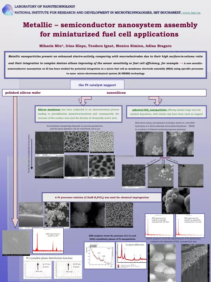
diameters. 10 – 30 nm. 100 – 200 nm. 70 – 100 nm. EDX spectrum for nanoPt on big SiO 2 nanoparticles (90 nm). EDX spectrum for nanoPt on small SiO 2 nanoparticles (18 nm). EDX spectrum for nanoPt on PS. In-plane diffraction. (a) 10 nm Si pores. (b) 30 nm Si pores. 26.8 nm. 29.2 nm.

E N D
diameters 10 – 30 nm 100 – 200 nm 70 – 100 nm EDX spectrum for nanoPt on big SiO2 nanoparticles (90 nm) EDX spectrum for nanoPt on small SiO2 nanoparticles (18 nm) EDX spectrum for nanoPt on PS In-plane diffraction (a) 10 nm Si pores (b) 30 nm Si pores 26.8 nm 29.2 nm (a) (b) LABORATORY OF NANOTECHNOLOGY NATIONAL INSTITUTE FOR RESEARCH AND DEVELOPMENT IN MICROTECHNOLOGIES, IMT BUCHAREST, www.imt.ro Metallic – semiconductor nanosystem assembly for miniaturized fuel cell applications Mihaela Miu*, Irina Kleps, Teodora Ignat, Monica Simion, Adina Bragaru * mihaela.miu@imt.ro Metallic nanoparticles present an enhanced electro-activity comparing with macroelectrodes due to their high surface-to-volume ratio and their integration in complex devices allows improving of the sensor sensitivity or fuel cell efficiency, for example→A new metallic-semiconductor nanosystem on Si has been studied for potential integration in a micro fuel cell as membrane electrode assembly (MEA) using specific processes to nano- micro-electromechanical system (N/MEMS) technology the Ptcatalyst support polished silicon wafer nanosilicon 1 2 Silicon membrane has been subjected to an electrochemical process leading to porosification (nanostructuration) and consequently the increase of the surface area and the density of chemically active sites spherical SiO2 nanoparticlesoffering similar huge area for catalyst deposition, with similar size have been used as support fabricated using a precipitation technique based on controlled hydrolysis of a silicon alkoxide (tetraethylorthosilicate - TEOS) in a mixture of ethanol containing aqueous ammonia. Si membrane morphology depends on process parameters, and the pores diameter can be tuned from nm to µm From few nm to hundreeds of nm pores A Pt precursor solution (3.5mM H2PtCl6) was used for chemical impregnation XRD analyses reveal the presence of (111) and (200) crystallinity phases of Pt nanoparticles EDAX analyses reveal the improvement of Pt distribution related to the diminish of SiO2 nanoparticle size Pt crystallite phase distribution function