Download
1 / 32
320 likes | 340 Views
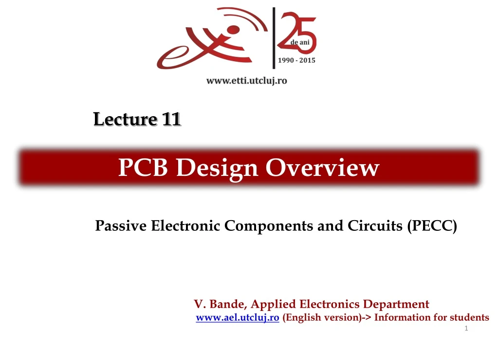
Lecture 11. PCB Design Overview. Passive Electronic Components and Circuits ( PECC ). PCB Design Overview. Electronic Packaging Levels PCB Design Principles The Electrical Model of the Interconnecting Structure. Electronic Packaging Levels.

E N D
Lecture 11 PCB Design Overview Passive Electronic Components and Circuits (PECC)
PCB Design Overview Electronic Packaging Levels PCB Design Principles The Electrical Model of the Interconnecting Structure
Electronic Packaging Levels • The electronic packaging is a trans-disciplinary domain which combines engineering with the fabrication technologies needed to transform an electric schematic design in a functional assembly. This domain combines knowledge from electronics, mechanics, material sciences and involves also quality control procedures. • The microsystem’s electronic packaging includes a fundamental technology set as follows: micro and nano-electronics, photonics, micro – electro – mechanical systems (MEMS), radio frequency (RF) and also wireless technology. For those functions to work properly inside a system, a designing procedure must be implemented, then fabrication, testing, thermal analyzed and also liability measures must be taken into consideration.
Electronic Packaging Levels • Level 0: Interconnections at the semiconductor substrate level. • Level 1: Chip’s encapsulation. • Level 2: Multi-chip modules design. • Level 3: PCB Design. • Level 4: Electronic and mechanical assemblies interconnection at the final system’s level (PCB’s, trays, slots, casings).
Electronic Packaging Levels Dies Silicon or germanium wafer Level 1 Integrated Circuit Level 2 Multichip module Level 3 PCB Level 4 System
Electronic Packaging Levels • Level 0: Interconnections at the semiconductor substrate level. • The interconnections made inside a chip are not considered (in a common situation) to represent an electronic packaging level.
Electronic Packaging Levels • Level 1: Chip’s encapsulation – Single Chip Module (SCM) Through Hole Package Surface Mounted Package DIP – Dual In-line Package SOP – Small Outline Package SOG SOJ SH-DIP (Shrink DIP) QFP – Quad Flat Package SK-DIP or SL-DIP (Skinny) LCC – Leadless Chip Carrier SIP – Single In-line Package BGA – Ball Grid Array ZIP – Zig-zag In-line Package CSP – Chip Scale Package PGA – Pin Grid Array
Electronic Packaging Levels • Level 2: Multi chip modules (MCM). • MCM-D – technology which uses a deposited dielectric film (deposited thin-film multilayers). • MCM-C – technology which uses a ceramic based dielectric (thick film or co-fired ceramic technology). Example: LTCC – low temperature co-fired ceramic). • MCM-L – technology which uses a laminated dielectric (organic laminate technology).
Electronic Packaging Levels • Level 3: Printed Circuit Boards – PCB or Printed Wiring Board - PWB • Paul Eisler – the inventor of the PCB technology in 1943. • The annual industry production world-wide is around 45.250 millions dollars with annual growth rate of 11%. • The most important producers realizes (each one of them!) app. 250.000 square meters of PCBs, the small ones around 50.000 square meters.
Electronic Packaging Levels • Level 4: System level – can comprise: • PCBs. • Assemblies: power sources, micro-motors, etc. • Userinterface elements: displays, keyboards, etc. • Special components: transformers, fans, sinks, etc. • Cables or connection wires. • Trays, slots, boxes, protection casings, etc.
PCB Design Overview Electronic Packaging Levels PCB Design Principles The Electrical Model of the Interconnecting Structure
PCB Design Principles • Printed Circuit Boards – PCB or Printed Wiring Board - PWB • The most important electronic packaging level! • With the help of copper traces, different components or integrated circuits around a PCB are being interconnected. • A PCB can be also viewed as a mechanical stand for the components.
PCB Design Principles • Printed Circuit Boards – PCB or Printed Wiring Board - PWB • Most important characteristics: • The width of the interconnection traces. • The pitch – center-to-center dimension between pins or pads. • The pad number – used for components on every square centimeter. • The via dimension – the diameter of the metalized holes from a layer to another. • The layers number – on which the interconnection traces are being made.
PCB Design Principles • Printed Circuit Boards – PCB or Printed Wiring Board - PWB • Technological landmarks: Trace width Technology Substrate Rigid Single layer 1985: 500µm Double layer Flexible 1990-1995: 250µm Multi layer Rigid-Flexible 1995-2000: 150µm Multi layer with micro-via and high density 3D Boards 2000-2005: 100µm 2003-2006: 75µm 2005-2008: 50µm 2008-2010: 30µm
PCB Design Principles • Printed Circuit Boards – PCB or Printed Wiring Board - PWB • Drilling – the most restrictive (expensive) operation!
PCB Design Principles • Single-layer PCBs – Technological Steps Debiting the laminated board. Printing the circuit geometry (screen printing) using photo or serigraphy technology. Etching (ro. “corodare”) – chemical or mechanical. Tin covering for protection purposes. (roller tinning) Drilling.
PCB Design Principles • Double-layer PCBs – Technological Steps Debiting the laminated board. Drilling. Holes metallization (through hole plating). Printing the circuit geometry (dry film printing) using photo-resistive technology. Tin covering for protection purposes. (roller tinning) Photo-resistive material removing. Etching (ro. “corodare”). Mask depositing (solder-mask, silk-screen, etc.)
PCB Design Principles • Multi-layer PCBs – Technological Steps Inner layers are being realized following the technological steps for single or double layers PCBs (without the mask depositing step) The inner layers are being treated with an adhesive substance, afterwards are being laminated together with the two exterior layers (Top and Bottom). The two exterior layers are fully covered by copper. The resulted multi-layer PCB is now processed as a double-sided PCB.
PCB Design Principles • Example: Double-layer PCB
PCB Design Principles • Example: Non-electric layers (CAD) SOLDER MASK LAYER SOLDER PASTE LAYER ASSEMBLY LAYER SILKSCREEN TOP
PCB Design Principles • Example: Fully equipped PCB
PCB Design Overview Electronic Packaging Levels PCB Design Principles The Electrical Model of the Interconnecting Structure
The Electrical Model of the Interconnecting Structure • The capacitance between two parallel traces – Case 1 • If d/w<<1, then Kc=1
The Electrical Model of the Interconnecting Structure • The Fringing Capacitance - Kc
The Electrical Model of the Interconnecting Structure • The capacitance between two parallel traces – Case 2
The Electrical Model of the Interconnecting Structure • The electrical equivalent relative permittivity – εr(eff) • The electrical equivalent relative permittivity is the result of pacing the conductive traces inside a non-homogenous dielectric environment. This parameter’s value can be calculated taking into consideration the substrate’s relative permittivity value, respective the capacitor’s geometrical dimensions.
The Electrical Model of the Interconnecting Structure • The capacitance between two parallel traces – Case 2 (particularities) • For two traces with different widths • For d>>w
The Electrical Model of the Interconnecting Structure • The capacitance between a trace superposed over a ground plane
The Electrical Model of the Interconnecting Structure • The capacitance between two traces superposed over a ground plane
The Electrical Model of the Interconnecting Structure • The inductivity of two traces with a rectangular section – Case A
The Electrical Model of the Interconnecting Structure • The inductivity of two traces with a rectangular section – Case B
The Electrical Model of the Interconnecting Structure • The inductivity of a trace superposed over a ground plane