Download

1 / 20
210 likes | 243 Views
Learn the structured approach to RTL design using VHDL code, block diagrams, ASM charts, and testing. Understand the execution unit, control signals, datapath, and controller components in detail.

E N D
Lecture 9 RTL Design Methodology
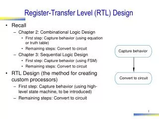
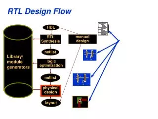
Structure of a Typical Digital System Data Inputs Control Inputs Control Signals Datapath (Execution Unit) Controller (Control Unit) Status Signals Data Outputs Control Outputs
Hardware Design with RTL VHDL Interface Pseudocode Datapath Controller Block diagram State diagram or ASM chart Block diagram VHDL code VHDL code VHDL code
Steps of the Design Process • Text description • Interface • Pseudocode • Block diagram of the Datapath • Interface with the division into the Datapath and the Controller • ASM chart of the Controller • RTL VHDL code of the Datapath, the Controller, and the Top Unit • Testbench of the Datapath, the Controller, and the Top Unit • Functional simulation and debugging • Synthesis and post-synthesis simulation • Implementation and timing simulation • Experimental testing
Steps of the Design ProcessPracticed in Class Today • Text description • Interface • Pseudocode • Block diagram of the Datapath • Interface with the division into the Datapath and the Controller • ASM chart of the Controller • RTL VHDL code of the Datapath, the Controller, and the Top Unit • Testbench of the Datapath, the Controller, and the Top Unit • Functional simulation and debugging • Synthesis and post-synthesis simulation • Implementation and timing simulation • Experimental testing
min_max_average example
Circuit Interface clk DONE reset n n in_data out_data 5 MIN_MAX_AVR 2 in_addr out_addr write START
Pseudocode Begin: wait for START; MAX = 0; MIN = 2n-1; SUM = 0; for i=0 to 31 do CDATA = M[i]; SUM = SUM + CDATA; if (CDATA < MIN) then MIN = CDATA; endif if (CDATA > MAX) then MAX = CDATA; endif endfor AVR = SUM/32 DONE = 1 goto Begin
Difference between a regular flowchart and ASM chart: Transition governed by clock Transition done between ASM blocks Basic rules: For a given input combination, there is one unique exit path from the current ASM block The exit path of an ASM block must always lead to a state box. The state box can be the state box of the current ASM block or a state box of another ASM block. Chapter 10
Incorrect ASM charts: Chapter 10
sorting example
Sort Clock Resetn N N DataIn DataOut L RAdd Done WrInit S (0=initialization 1=computations) Rd Sorting - Required Interface
Simulation results for the sort operation (1)Loading memory and starting sorting
Simulation results for the sort operation (2)Completing sorting and reading out memory
Sorting - Example During Sorting After sorting Before sorting i=0 i=0 i=0 i=1 i=1 i=2 j=1 j=2 j=3 j=2 j=3 j=3 Address 0 1 2 3 3 3 2 2 1 1 1 1 2 2 3 3 3 3 2 2 4 4 4 4 4 4 4 3 1 1 1 1 2 2 3 4 Legend: position of memory indexed by i position of memory indexed by j Mj Mi
Pseudocode wait for s=1 for i=0 to k-2 do A = Mi for j=i+1 to k-1 do B = Mj if A > B then Mi = B Mj = A A = Mi end if end for end for Done wait for s=0 go to the beginning
DataIn RAdd 0 ABMux N L L N LD Li Resetn 1 0 s EN RST Ei CLK Din Clock s +1 Csel WrInit DIN We LD Lj WE 0 Resetn L Addr EN RST i Ej Wr ADDR 0 CLK Clock CLK 1 Clock L L j DOUT 1 N ABData EN RST = k-1 CLK Ben Aen = k-2 Resetn Resetn EN RST CLK Clock Clock Rd zi N zj N N Bout 0 1 B A DataOut A>B AgtB Block diagram of the Execution Unit