Download
1 / 39
480 likes | 1.36k Views
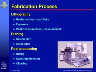
Simplified Example of a LOCOS Fabrication Process. Prof. A. Mason Electrical and Computer Engineering Michigan State University. LOCOS Defined. LOCOS = LOCal Oxidation of Silicon Defines a set of fabrication technologies where the wafer is masked to cover all active regions

E N D
Simplified Example of aLOCOS Fabrication Process Prof. A. Mason Electrical and Computer Engineering Michigan State University Prof. A. Mason
LOCOS Defined • LOCOS = LOCal Oxidation of Silicon • Defines a set of fabrication technologies where • the wafer is masked to cover all active regions • thick field oxide (FOX) is grown in all non-active regions • Used for electrical isolation of CMOS devices • Relatively simple to understand so often used to introduce/describe CMOS fabrication flows • Not commonly used in modern fabrication • other techniques, such as Shallow Trench Isolation (STI) are currently more common than LOCOS Prof. A. Mason
LOCOS –step 1 Form N-Well regions • Grow oxide • Deposit photoresist NWELL mask photoresist oxide p-type substrate Cross section view NWELL mask Layout view Prof. A. Mason
LOCOS –step 1 Form N-Well regions • Grow oxide • Deposit photoresist • Pattern photoresist • NWELL Mask • expose only n-well areas NWELL mask photoresist oxide p-type substrate Cross section view NWELL mask Layout view Prof. A. Mason
LOCOS –step 1 Form N-Well regions • Grow oxide • Deposit photoresist • Pattern photoresist • NWELL Mask • expose only n-well areas • Etch oxide • Remove photresist oxide p-type substrate Cross section view Layout view Prof. A. Mason
LOCOS –step 1 Form N-Well regions • Grow oxide • Deposit photoresist • Pattern photoresist • NWELL Mask • expose only n-well areas • Etch oxide • Remove photoresist • Diffuse n-type dopants through oxide mask layer n-well p-type substrate Cross section view Layout view Prof. A. Mason
LOCOS –step 2 Form Active Regions • Deposit SiN over wafer • Deposit photoresist over SiN layer ACTIVE mask n-well photoresist SiN p-type substrate ACTIVE mask Prof. A. Mason
LOCOS –step 2 Form Active Regions • Deposit SiN over wafer • Deposit photoresist over SiN layer • Pattern photoresist • *ACTIVE MASK ACTIVE mask n-well photoresist SiN p-type substrate ACTIVE mask Prof. A. Mason
LOCOS –step 2 Form Active Regions • Deposit SiN over wafer • Deposit photoresist over SiN layer • Pattern photoresist • *ACTIVE MASK • Etch SiN in exposed areas • leaves SiN mask which blocks oxide growth n-well photoresist SiN p-type substrate ACTIVE mask Prof. A. Mason
LOCOS –step 2 Form Active Regions • Deposit SiN over wafer • Deposit photoresist over SiN layer • Pattern photoresist • *ACTIVE MASK • Etch SiN in exposed areas • leaves SiN mask which blocks oxide growth • Remove photoresist • Grow Field Oxide (FOX) • thermal oxidation n-well FOX p-type substrate ACTIVE mask Prof. A. Mason
LOCOS –step 2 Form Active Regions • Deposit SiN over wafer • Deposit photoresist over SiN layer • Pattern photoresist • *ACTIVE MASK • Etch SiN in exposed areas • leaves SiN mask which blocks oxide growth • Remove photoresist • Grow Field Oxide (FOX) • thermal oxidation • Remove SiN n-well FOX p-type substrate ACTIVE mask Prof. A. Mason
LOCOS –step 3 Form Gate (Poly layer) • Grow thin Gate Oxide • over entire wafer • negligible effect on FOX regions gate oxide Prof. A. Mason
LOCOS –step 3 Form Gate (Poly layer) • Grow thin Gate Oxide • over entire wafer • negligible effect on FOX regions • Deposit Polysilicon • Deposit Photoresist POLY mask polysilicon gate oxide POLY mask Prof. A. Mason
LOCOS –step 3 Form Gate (Poly layer) • Grow thin Gate Oxide • over entire wafer • negligible effect on FOX regions • Deposit Polysilicon • Deposit Photoresist • Pattern Photoresist • *POLY MASK • Etch Poly in exposed areas • Etch/remove Oxide • gate protected by poly POLY mask gate oxide POLY mask Prof. A. Mason
LOCOS –step 3 Form Gate (Poly layer) • Grow thin Gate Oxide • over entire wafer • negligible effect on FOX regions • Deposit Polysilicon • Deposit Photoresist • Pattern Photoresist • *POLY MASK • Etch Poly in exposed areas • Etch/remove Oxide • gate protected by poly gate oxide Prof. A. Mason
LOCOS –step 4 Form pmos S/D • Cover with photoresist PSELECT mask PSELECT mask Prof. A. Mason
LOCOS –step 4 Form pmos S/D • Cover with photoresist • Pattern photoresist • *PSELECT MASK PSELECT mask POLY mask Prof. A. Mason
LOCOS –step 4 Form pmos S/D • Cover with photoresist • Pattern photoresist • *PSELECT MASK • Implant p-type dopants • Remove photoresist p+ dopant p+ dopant POLY mask Prof. A. Mason
LOCOS –step 5 Form nmos S/D • Cover with photoresist NSELECT mask p+ p+ p+ n POLY mask Prof. A. Mason
LOCOS –step 5 Form nmos S/D • Cover with photoresist • Pattern photoresist • *NSELECT MASK NSELECT mask p+ p+ p+ n POLY mask Prof. A. Mason
LOCOS –step 5 Form nmos S/D • Cover with photoresist • Pattern photoresist • *NSELECT MASK • Implant n-type dopants • Remove photoresist n+ n+ n+ p+ p+ p+ n n+ dopant n+ dopant POLY mask Prof. A. Mason
LOCOS –step 6 Form Contacts • Deposit oxide • Deposit photoresist CONTACT mask n+ n+ n+ p+ p+ p+ n CONTACT mask Prof. A. Mason
LOCOS –step 6 Form Contacts • Deposit oxide • Deposit photoresist • Pattern photoresist • *CONTACT Mask • One mask for both active and poly contact shown CONTACT mask n+ n+ n+ p+ p+ p+ n CONTACT mask Prof. A. Mason
LOCOS –step 6 Form Contacts • Deposit oxide • Deposit photoresist • Pattern photoresist • *CONTACT Mask • One mask for both active and poly contact shown • Etch oxide n+ n+ n+ p+ p+ p+ n Prof. A. Mason
LOCOS –step 6 Form Contacts • Deposit oxide • Deposit photoresist • Pattern photoresist • *CONTACT Mask • One mask for both active and poly contact shown • Etch oxide • Remove photoresist • Deposit metal1 • immediately after opening contacts so no native oxide grows in contacts • Planerize • make top level n+ n+ n+ p+ p+ p+ n Prof. A. Mason
LOCOS –step 7 METAL1 mask Form Metal 1 Traces • Deposit photoresist n+ n+ n+ p+ p+ p+ n METAL1 mask Prof. A. Mason
LOCOS –step 7 METAL1 mask Form Metal 1 Traces • Deposit photoresist • Pattern photoresist • *METAL1 Mask n+ n+ n+ p+ p+ p+ n METAL1 mask Prof. A. Mason
LOCOS –step 7 Form Metal 1 Traces • Deposit photoresist • Pattern photoresist • *METAL1 Mask • Etch metal n+ n+ n+ p+ p+ p+ n metal over poly outside of cross section Prof. A. Mason
LOCOS –step 7 Form Metal 1 Traces • Deposit photoresist • Pattern photoresist • *METAL1 Mask • Etch metal • Remove photoresist n+ n+ n+ p+ p+ p+ n Prof. A. Mason
LOCOS –step 8 VIA mask Form Vias to Metal1 • Deposit oxide • Planerize oxide • Deposit photoresist n+ n+ n+ p+ p+ p+ n VIA mask Prof. A. Mason
LOCOS –step 8 VIA mask Form Vias to Metal1 • Deposit oxide • Planerize • Deposit photoresist • Pattern photoresist • *VIA Mask n+ n+ n+ p+ p+ p+ n VIA mask Prof. A. Mason
LOCOS –step 8 Form Vias to Metal1 • Deposit oxide • Planerize • Deposit photoresist • Pattern photoresist • *VIA Mask • Etch oxide • Remove photoresist n+ n+ n+ p+ p+ p+ n Prof. A. Mason
LOCOS –step 8 Form Vias to Metal1 • Deposit oxide • Planerize • Deposit photoresist • Pattern photoresist • *VIA Mask • Etch oxide • Remove photoresist • Deposit Metal2 n+ n+ n+ p+ p+ p+ n Prof. A. Mason
LOCOS –step 9 METAL2 mask Form Metal2 Traces • Deposit photoresist n+ n+ n+ p+ p+ p+ n METAL2 mask Prof. A. Mason
LOCOS –step 9 METAL2 mask Form Metal2 Traces • Deposit photoresist • Pattern photoresist • *METAL2 Mask n+ n+ n+ p+ p+ p+ n METAL2 mask Prof. A. Mason
LOCOS –step 9 Form Metal2 Traces • Deposit photoresist • Pattern photoresist • *METAL2 Mask • Etch metal n+ n+ n+ p+ p+ p+ n Prof. A. Mason
LOCOS –step 9 Form Metal2 Traces • Deposit photoresist • Pattern photoresist • *METAL2 Mask • Etch metal • Remove photoresist n+ n+ n+ p+ p+ p+ n Prof. A. Mason
LOCOS –step 10+ Form Additional Traces • Deposit oxide • Deposit photoresist • Pattern photoresist • Etch oxide • Deposit metal • Deposit photresist • Pattern photoresist • Etch metal • Repeat for each additional metal n+ n+ n+ p+ p+ p+ n p-type substrate Prof. A. Mason
Simplifications from complete process • skipped several substrate doping steps • channel implant to adjust threshold voltages • surface implant to increase breakdown voltage • no LDD, lightly-doped drain • no deposition of contact interface materials • metal patterning simplified • more complex “lift-off” process often used • no overglass (thick top dielectric) layer • no bonding pad layer • simplified use of dark/clear field masks and positive/negative photoresist Prof. A. Mason