Download
1 / 2
30 likes | 217 Views
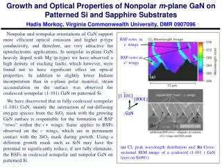
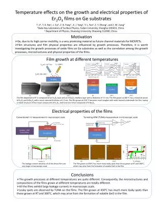
Growth and Optical Properties of Nonpolar m -plane GaN on Patterned Si and Sapphire Substrates Hadis Morko ç , Virginia Commonwealth University, DMR 0907096.

E N D
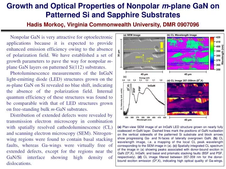
Growth and Optical Properties of Nonpolarm-plane GaN on Patterned Si and Sapphire Substrates HadisMorkoç, Virginia Commonwealth University, DMR 0907096 NonpolarGaN is very attractive for optoelectronic applications because it is expected to provide enhanced emission efficiency owing to the absence of polarization field. We have established a set of growth parameters to pave the way for nonpolarm-plane GaN layers on patterned Si(112) substrates. Photoluminescence measurements of the InGaN light-emitting diode (LED) structures grown on the m-plane GaN on Si revealed no blue shift, indicating the absence of the polarization field. Internal quantum efficiencyof these structures was found to be comparable with that of LED structures grown on free-standing bulk m-GaN substrates. Distribution of extended defects were revealed by transmission electron microscopy in combination with spatially resolved cathodoluminescence (CL) and scanning electron microscopy (SEM). Nitrogen-wing regions were found to contain basal stacking faults, whereas Ga-wings were virtually free of extended defects, except for the regions near the GaN/Si interface showing high density of dislocations. O Ba Sr Si (a) Plan-view SEM image of an InGaN LED structure grown on nearly fully coalesced m-GaN layer. Dashed lines mark the positions of GaN nucleation on the vertical sidewalls of the patterned Si substrate and block arrows show progressing Ga- and N-faces of laterally overgrown GaN. (b) CL wavelength image, i.e. a mapping of the local CL peak wavelength corresponding to the SEM image in (a). (c) Spatially integrated CL spectrum of the image in (a) showing peaks associated with donor-bound exciton in GaN (D0,X), InGaN, and basal and prismatic stacking faults (BSF and PSF, respectively). (d) CL image filtered between 357-359 nm for the donor-bound exciton emission (D0,X), indicating high optical quality of Ga-wings.
Growth and Optical Properties of Nonpolarm-plane GaN on Patterned Si and Sapphire Substrates HadisMorkoç, Virginia Commonwealth University, DMR 0907096 Interaction of the students from different universities provides them with different perspectives and teaches them the value of working in collaborative groups. The project was performed in strong collaborations with groups from the US and international universities. TEM experiments have been performed by Prof. D. J. Smith’s group at Arizona State University, and spatially resolved CL measurements were done by Prof. JürgenChristen’s group at the Otto-von-Guericke Universitat Magdeburg, Germany. A student exchange program is initiated as a result of this collaborative effort, where a graduate student from Universitat Magdeburg, Sebastian Metzner, will visit VCU for a period of year starting at the end of 2010. A student from VCU will also spend some time in Magdeburg. Graduate student Xing Li (right) operates the MOCVD system for m-plane GaN growth on patterned Si substrate