Download
1 / 50
500 likes | 610 Views
The WRAMP Processor. Next Topic: Processor Structures. Moving from the abstraction of a high level language (e.g.C) to the assembly language level allows a certain appreciation of the structure of a computer.

E N D
The WRAMP Processor COMP 201
Next Topic: Processor Structures • Moving from the abstraction of a high level language (e.g.C) to the assembly language level allows a certain appreciation of the structure of a computer. • This next module takes a look at some specific circuits, modeled in an abstract way, to provide some insight about HOW data moves around inside a processor. COMP 201
Processor Structures • Introduction • The CPU must perform three main tasks: • Communication with memory • Fetching Instructions • Fetching and storing data • Interpretation of Instructions • Execution of Instructions Processor System Bus I/O Memory COMP 201
Von Neumann Architecture • John von Neumann is credited with • Stored Program concept • Logical Organization, the “codes” by which a fixed system of wiring could solve a great variety of problems. • In other words a general purpose computer controlled by a computer program • Implicit separation between CPU and storage • Data and Instructions stored together COMP 201
Fetch-Decode-Execute Cycle • The CPU is endlessly looping through these steps • Actual steps will vary from processor to processor • Typical steps 1. instruction fetch & Program Counter update 2. instruction decode & operand load 3. operation execution (control instructions update Program Counter) 4. memory access 5. register update COMP 201
Instruction Cycle • Fetch the next instruction • If everything is normal • execute the instruction • increment PC • Otherwise, halt • This is a simplification • varied length instructions • multiple memory accesses • pipelining • Which line could cause HALT = true? //Load program PC = startAddress; HALT = BRANCH = false; //Instruction cycle IR = memory[PC]; while (!HALT){ PC++; execute(IR); IR = memory[PC]; } COMP 201
PC IR $3 $4 lw $3, 1005 1000 lw $4, 1006 add $3, $3, $4 sw $3, 1020 j 1000 j 984 3 0 21 12 0 false Instruction Cycle 1000 1001 1002 1003 1004 1005 1006 1007 HALT //Load program PC = startAddress; HALT = false; //Instruction cycle IR = memory[PC]; while (!HALT){ PC++; execute(IR); IR = memory[PC]; } Suppose the CPU just executed “j 1000”, the jump instruction. This changed the PC to 1000 and set the BRANCH flag. COMP 201
PC IR $3 $4 lw $3, 1005 1000 lw $4, 1006 add $3, $3, $4 sw $3, 1005 lw $3, 1005 j 984 3 0 21 12 0 false Instruction Cycle 1000 1001 1002 1003 1004 1005 1006 1007 HALT //Load program PC = startAddress; HALT = false; //Instruction cycle IR = memory[PC]; while (!HALT){ PC++; execute(IR); IR = memory[PC]; } Now the instruction register contains the word of data starting at memory location 1000. The 32 bits represent a load word instruction. COMP 201
PC IR $3 $4 lw $3, 1005 1001 lw $4, 1006 add $3, $3, $4 sw $3, 1005 lw $3, 1005 j 984 3 0 21 12 0 false Instruction Cycle 1000 1001 1002 1003 1004 1005 1006 1007 HALT //Load program PC = startAddress; HALT = false; //Instruction cycle IR = memory[PC]; while (!HALT){ PC++; execute(IR); IR = memory[PC]; } The program counter (PC) is incremented before an instruction is executed. COMP 201
PC IR $3 $4 lw $3, 1005 1001 lw $4, 1006 add $3, $3, $4 sw $3, 1005 lw $3, 1005 j 984 3 3 21 12 0 false Instruction Cycle 1000 1001 1002 1003 1004 1005 1006 1007 HALT //Load program PC = startAddress; HALT = false; //Instruction cycle IR = memory[PC]; while (!HALT){ PC++; execute(IR); IR = memory[PC]; } The data stored in the word beginning at memory address 1005 is stored in register $3. COMP 201
PC IR $3 $4 lw $3, 1005 1001 lw $4, 1006 add $3, $3, $4 sw $3, 1005 lw $4, 1006 j 984 3 3 21 12 0 false Instruction Cycle 1000 1001 1002 1003 1004 1005 1006 1007 HALT //Load program PC = startAddress; HALT = false; //Instruction cycle IR = memory[PC]; while (!HALT){ PC++; execute(IR); IR = memory[PC]; } The next instruction is fetched. COMP 201
PC IR $3 $4 lw $3, 1005 1002 lw $4, 1006 add $3, $3, $4 sw $3, 1005 lw $4, 1006 j 984 3 3 21 12 0 false Instruction Cycle 1000 1001 1002 1003 1004 1005 1006 1007 HALT //Load program PC = startAddress; HALT = false; //Instruction cycle IR = memory[PC]; while (!HALT){ PC++; execute(IR); IR = memory[PC]; } The program counter (PC) is incremented before an instruction is executed. COMP 201
PC IR $3 $4 lw $3, 1005 1001 lw $4, 1006 add $3, $3, $4 sw $3, 1020 lw $4, 1006 j 984 3 3 21 12 21 false Instruction Cycle 1000 1001 1002 1003 1004 1005 1006 1007 HALT //Load program PC = startAddress; HALT = false; //Instruction cycle IR = memory[PC]; while (!HALT){ PC++; execute(IR); IR = memory[PC]; } The contents of memory location 1006 are stored in register $4. COMP 201
Processor Structures • There are many possible ways of putting a CPU together. However, four main building blocks are used to construct a CPU: • These are controlled by the state machine • Registers • ALUs • Memory Interface • Buses Sometimes termed the Datapath COMP 201
Processor Building Blocks • Registers: local storage within the CPU • ALU - Arithmetic Logic Unit: performs arithmetic and logic operations • Memory Interface: to load instructions and data • Buses: connect the other parts together COMP 201
Registers • Both the general purpose registers and special purpose registers for the WRAMP processor are constructed of D-type Flip-Flops, one for each bit in the register. Functional representation Data Out Control 32 control D Q register D inn control D outn clk Clk Enable control 32 Data In COMP 201
Registers (continued) • In order to minimize connections and circuitry used to move data from one place to another within the processor, data paths are shared using a bus system. • Signals are used to control what device is using the data path at any given time; these are termed “control lines” • The switch shown on the preceeding slide is functional only; in fact, a “tri-state output” is used, to prevent circuit malfunction which would occur if two devices were to drive the bus at the same time. COMP 201
B Bout SELB SELC Cin SELA Aout Registers (continued) • General purpose registers contained within a register file • Want to be able to output two operands and receive result at the same time C B C 32 32 SELA Reg File (R0-R15) R0 Aout R1 SELB ... Bout R15 SELC Cin 32 NOTE: SELx are control lines A A COMP 201
Carries out arithmetic and logic operations as commanded by the control unit out = A func B . arithmetic Bitwise &misc Test/ set add addu sub subu mult multu div divu rem remu sll and srl or sra Xor lhi inc slt sltu sgt sgtu sle sleu sge segu seq sequ sne sneu ALU Functions within WRAMP func A n All data paths 32 bits! out B ALUoe Controls when output from ALU is placed on common data bus COMP 201
operation op a b res result An ALU (arithmetic logic unit) • build an ALU to support the andi and ori instructions • we'll just build a 1 bit ALU, and use 32 of them • Possible Implementation (sum-of-products): a b COMP 201
S A C B Review: The Multiplexor • Selects one of the inputs to be the output, based on a control input • Lets build our ALU using a MUX: 0 1 note: we call this a 2-input mux even though it has 3 inputs! COMP 201
Different Implementations • Not easy to decide the “best” way to build something • Don't want too many inputs to a single gate • Dont want to have to go through too many gates • for our purposes, ease of comprehension is important • Let's look at a 1-bit ALU for addition: • How could we build a 1-bit ALU for add, and, and or? • How could we build a 32-bit ALU? cout = a b + a cin + b cin sum = a xor b xor cin COMP 201
Full adder circuit A B Sum Cout Cin Sum = Cin xor A xor B Cout = A.B + A.Cin + B.Cin COMP 201
Building a 32 bit ALU COMP 201
What about subtraction (a – b) ? • Two's complement approch: just negate b and add. • How do we negate? • A very clever solution: COMP 201
Test for equality • Notice control lines:000 = and001 = or010 = add110 = subtract111 = slt • Note: zero is a 1 when the result is zero! COMP 201
ALU Conclusion • We can build an ALU to support the WRAMP instruction set • key idea: use multiplexor to select the output we want • can efficiently perform subtraction using two’s complement • can replicate a 1-bit ALU to produce a 32-bit ALU • Important points about hardware • the speed of a circuit is affected by the number of gates in series (on the “critical path” or the “deepest level of logic”) • Clever changes to organization can improve performance (similar to using better algorithms in software) COMP 201
Memory Interface • Interacts with memory to fetch instructions and read or write data • Must have some way of initiating memory read and write cycles read write Data out Data in Memory MI All data paths 32 bits! Address COMP 201
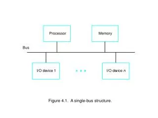
Buses—General considerations • Connect together the components of the processor. Different numbers of buses can be used to form different architectures • Consider first: single bus structure • only one data transfer can occur at a time • need extra temporary registers (e.g. T1 & T2) Memory A MI PC Reg File (R0-R31) T2 T1 B COMP 201
To be more specific, consider an instruction fetch. • In an instruction fetch, the contents of the program counter (PC) are used to “point” to a location in memory, where the next instruction is resident. Then, the contents of that location are written to the instruction register (IR). In a single bus system, there will need to be some buffer register associated with memory, to hold the address, while the data is fetched. So instruction fetch takes three cycles: • PC count onto bus, to be saved in the MAR (memory address register) • Data from the memory address to bus, copied into IR • PC incremented to point at next instruction COMP 201
Memory MAR A MI PC Reg File (R0-R31) T2 IR T1 B Memory MAR A Memory MI A PC Reg File (R0-R31) T2 IR T1 MI PC Reg File (R0-R31) T2 IR T1 Memory MAR B A MI B PC Reg File (R0-R31) T2 IR T1 Memory MAR A MI B PC Reg File (R0-R31) T2 IR T1 B Pictorial—Instruction fetch COMP 201
Buses (continued) • Two bus structure • This structure is common for microcontrollers and microprocessors, e.g. 8051. Some data transfers require several steps and temp registers. Data Bus Memory A C A MI PC Reg File (R0-R31) T2 T1 ALU B B Address Bus COMP 201
C Bus B Bus Memory A C A MI TEMP PC IR Reg File (R0-R15) ALU B B A bus Buses (continued) • Three bus structure, as used on WRAMP • Three bus transfers can take place at same time • Two operand buses and a result bus or an address bus plus data bus for memory transfers. COMP 201
C Bus B Bus Memory MI TEMP PC IR Reg File (R0-R15) ALU A bus temp_out Some details we leave out of the drawings, for clarity • Actually, the routes to/from each element are controlled with switches, but are not shown. Nevertheless, when operating the simulator, you will need to realize what switch controls which dataflow element. For instance, temp_out controls when the temp register drives the A bus. COMP 201
Component Signal Name Description Register File a out Causes the contents of the register selected by sel a to be output onto the A bus. sel a Select which register will be output onto the Abus if a out is asserted. b out Causes the contents of the register selected by sel b to be output onto the B bus. sel b Select which register will be output onto the B bus if b out is asserted. c in Causes the value from the C bus to be written into the register selected by sel c. sel c Select which register to write the value from the C bus into when the c in signal is asserted. ALU alu out Causes the result of the current ALU function se- lected by alu func to be output to the C bus. alu func Defines the current operation that the ALU should perform. Memory Interface mem read Causes the contents of the memory address specified on the A bus to be read and output onto the C bus. mem write Causes the value on the B bus to be written into the memory address specified on the A bus. Descriptions of each of the control signals COMP 201
Signal descriptions (continued) Program Counter pc out Causes the contents of the PC register to be output onto the A bus. pc in Causes the value on the C bus to be written into the PC. Instruction imm 16 out Causes the least signi_cant 16 bits of the IR to Register be output onto the B bus. imm 20 out Causes the least signi_cant 20 bits of the IR to be output onto the B bus. sign extend Causes the output from the IR to be sign extended to 32bits. ir in Causes the value on the C bus to be written into the IR. Temp Register temp out Causes the contents of the temporary register to be output onto the A bus. temp in Causes the value on the C bus to be written into the temporary register. COMP 201
Sample WRAMP processor operations • Following are datapath drawings, showing which paths are used for which items of data, for common operations. • Colored lines depict main flow; black lines depict connections which are inactive. COMP 201
An instruction fetch • For an instruction fetch, the contents of the program counter (PC) must be sent to the memory, and the contents of the selected memory location loaded into the instruction register (IR). C bus Data B bus Memory A C A MI IR PC Reg File (R0-R15) ALU B Address B A bus COMP 201
An Addition • In WRAMP, an addition takes the contents of two registers, adds it, and places the result in another register. add $3, $4, $5 • And so, control signals route $4 and $5 to the ALU inputs, and the result from the ALU into $3. Memory A C A MI PC $3 ALU $4 B $5 B COMP 201
A memory operation • In WRAMP, a memory fetch requires two steps • compute the effective address • Apply the address to memory and perform the indicated operation (read or write) • Step one: compute effective address C Bus B Bus Memory MI TEMP PC IR Reg File (R0-R15) ALU A bus Whichever register used as base COMP 201
Memory operation (continued) • Then, the effective address is applied to A bus and through the memory interface to the Memory. The data at that address in memory is placed on the C bus, which is then routed to the destination register (e.g. $4) C Bus B Bus Memory MI TEMP PC IR $4 ALU Reg File (R0-R15) A bus COMP 201
WRAMP operations… a comparison • In a comparison, the ALU is used to determine if the specified condition exists… e.g. sgt Rd, Rs, Rt . • Rs is applied to input A, Rt is applied to input B and the output from the ALU is applied to Rd. C Bus B Bus Memory A MI TEMP PC IR $4 ALU $5 B $6 • Sgt $4, $5, $6 Reg File (R0-R15) A bus COMP 201
WRAMP operations…conditional branch • In a conditional branch, you must test the condition, and if the condition is met, change the contents of the PC from where it is now pointing (the next instruction in sequence) to the branch instruction (found in the lower 20 bits of the instruction). E.g. beqz $1, loop C Bus B Bus Memory A C A MI TEMP PC IR Reg File (R0-R15) ALU B You must examine result. And then do the second part… B A bus COMP 201
And then the second part, depending upon the result of part one: assume branch taken… Switches to set: pc_out, imm_20_out, sign_extend*, alu_out, alu_fcn= add, pc_in. *= does not matter C Bus B Bus Memory MI TEMP PC IR Reg File (R0-R15) ALU A bus COMP 201
C Bus B Bus Memory A C A MI TEMP PC IR Reg File (R0-R15) ALU B B A bus temp_out You may want to keep this slide handy, when working on the Exercise 4! COMP 201
As viewed on simulator, Switches to set: a_out sel_a=$0 sel_b=$1 b_out alu_out alu_func= add this indicates if the ALU is zero COMP 201
As viewed on simulator, Switches to set: pc_out imm_20_out sign_extend pc_in alu_out alu_func= add COMP 201
Processor Structures Summary • All computers use a Von Neumann architecture where instructions and data are stored in memory separate from the processor. • The processor works on an instruction fetch-decode-execute cycle. • The Program Counter keeps track of which instruction to load next. COMP 201
Processor Structures - Summary 2 • CPUs are made up of Registers, ALUs, Memory Interface and Buses. • There are temporary registers and the PC is a register as well as the general purpose registers. • The Instructions drive control lines to make the components perform the desired operation. COMP 201