Download
1 / 17
180 likes | 346 Views
Low Power Sensor Node Processor Architecture. G. Pani ć, T. Basmer. K. Tittelbach-Helmrich, L. Lopacinski. Outline. Introduction Motivation Processor System Architecture Implementation Conclusion. Introduction – Wireless Sensor Networks. Sensor Networks

E N D
Low Power Sensor Node Processor Architecture G. Panić, T. Basmer. K. Tittelbach-Helmrich, L. Lopacinski
Outline • Introduction • Motivation • Processor System Architecture • Implementation • Conclusion
Introduction – Wireless Sensor Networks • Sensor Networks A [wireless] network of low cost, densely deployed, untethered sensor nodes • Applications Industrial, Homeland Security, Telemedicine, Context Sensitive Systems
WSN – Sensor Node Modern Sensor Nodes UC Berkeley: COTS Dust IHP Tandem Stack UC Berkeley: Smart Dust UC Berkeley: COTS Dust Rockwell: WINS IHP Feuerwhere UCLA: WINS JPL: Sensor Webs
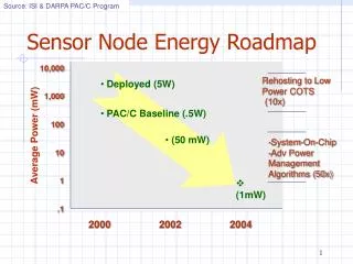
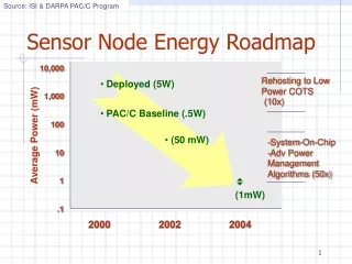
Motivation Memory General Goals: Design a sensor node platform for future WSN applications Low power processing Reuse flexibility Sensoric Processing Radio Sensor Node: Three basic op. units: Sensoric, Processing, Radio Memory for software Battery powered
Power Issues • The most important limitation factor isPOWER! [ITRS 2002]
Sensor Node – Power Optimization • High Level Of Integration single chip solution, MTCMOS • Optimized Node Architecture reduced on-chip communication, DMA, hardware accelerators • Advanced Power Saving Methodologies power gating, DFVS, multi-voltage design • Low Power Radio picoRadio, wake-up concept • Non-Standard Approach asynchronous logic, latch-based design, etc.
IHP Sensor Node Platform Retention MAC Hw Accelerator Baseband AFE Debug I/F CPU ROM Objectives: low power processing -> async CPU wireless connectivity -> BB, SPI sensor connectivity -> Digital I/O, SPI Wake-up Power Gating Controller RAM Data Storage Sensors A/D Preprocessor I/O Ports System Timer SPI Power-gating partitions Challenges: peripheral interface to async CPU peripheral register access glitch free control logic
Timer BB RAM IPMS 430x MUX SPI P1 P2 P3 P4 ROM Sensor Node – Processor Architecture • IPMS430x – low power asynchronous TI MSP430x clone, I2C debug port • Timer – 3 CAP/CMP regs, PWM, clock divider • Digital I/O – 2 simple I/Os and 2 with interrupt capability • SPI master – edge selection, burst mode • Baseband - DIN EN 13757-4, DSSS extended Debug (I2C)
csl_n p1_sel csh_n p1_clk delay Addr Latch Addr Demux address pn_sel pn_clk delay Implementation - RTL Peripheral Interface (Clock Generation) mclk addr csl_n csh_n px_sel outputs px_clk
glitch filter Reg File Ctrl Logic delay S R Implementation - RTL Glitch Filtering delay reg[0] reg[1] input set <= '1' when reg(1 downto 0) = "01" else '0'; reg[1:0] changes from "00" to "11" -> potential glitch delayed_input output
Implementation - RTL p_sel Peripheral Register Access periph_data 0 cpu_data 1 D 0 periph_clk cpu_clk 1 - cpu access has priority! - peripheral clock can be gated by software to avoid conflicts
Implementation - Synthesis post-synthesis results target frequency 20 MHz, worst case conditions
Implementation - Layout Size: 12,6 mm2 Nr. of Pads: 115 (91 sig, 24 p/g) Max Freq: 20 MHz Power (Core): 4-5 mW@20MHz The chip has been produced and successfully tested!
Results Comparison IHP IPMS430x vs Tmote Sky MSP430F1611
Conclusion • IPMS430x based system designed low power, low CPU core area, large address space (1MB) additional baseband functionality external Flash interface (disadvantage) • Design challenges resolved peripheral interface, glitch filtering, register access • Trade-Off implementation effort testability of asynchronous logic undiscovered errors on asynchronous paths • Future Work integration of additional components: Flash, DMA, AFE, etc. power gating implementation reduction of pads number
The End Thanx Any Questions???