Download

1 / 15
150 likes | 357 Views
B.G. Cheon (Hanyang U) Dec.10-12 @ KEK 1 st open meeting of the Super KEKB Collaboration. ECL trigger for Super Belle. Belle ECL physics triggers. Total Energy. Cluster Counting. Belle ECL Electronics. Super Belle ECL trigger electronics. SEQ. PD+ Preamp. GDL. Shaper.

E N D
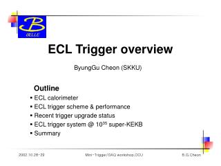
B.G. Cheon (Hanyang U) Dec.10-12 @ KEK 1st open meeting of the Super KEKB Collaboration ECL trigger for Super Belle
Belle ECL physics triggers Total Energy Cluster Counting
Super Belle ECL trigger electronics SEQ PD+ Preamp GDL Shaper Final trigger (23) analog sum (592) Gb serial link (52) FAM ( FADC+ FPGA) Gb serial link (52) TMM ( FPGAs) Monitor
Advantage of FAM + TMM scheme • Electronics chain will be very simple. • More flexible trigger algorithm design than Belle trigger. • Reduction of cable; lots of bulky copper cables 52 optical fibers • Simple monitoring scheme (extra QT & TDCs are not necessary) • Easy handling of CsI(Tl) and pure-CsI signals simultaneously
Flash ADC Trigger Module (FAM) • 52 FAMs to cover all the TC(4x4 crystals) signals. • Input : 12 TC analog sum signals from each shaper • Continuous Input signal digitization @ 100MS/s 12bit • Output : 12 TC <pulse height + discriminator bit> via Gbit link • TC output gain variation adjustment using look-up-table • One board(12 TC channels) / VME crate • Crystal gain adjustment will be done at shaper board.
New VME shaper-digitizer board Gain adjustment(4bit/crystal) + Analog-sum for trigger
Trigger & Monitoring Module (TMM) • Input : 52 x 12 TC signals from FAM modules • 7 FPGAs + VME interface • If all parts are not fitted into one board, partitioning & cascading design will be taken into account. • Output : 23 ECL final trigger signals to GDL 4 ECL trigger timings ( Final, Fwd, Barrel, Bwd ) 3 Total Energy ( >0.5, 1.0, 3.0 GeV) 4 Isolated Cluster Number ( 3 bits + 1 carry-bit) 11 types of Bhabha triggers 1 Cosmic Veto ** Any more useful trigger algorithm will be studied.
Timing Latency • Crystal to FAM = ~100ns • Peaking time=700ns @ peak position of analog sum signal • ADC pipeline latency @ FAM = ~100ns • Peak finding process @FAM = 100 ~ 200ns • Programmable delay @ FAM = ~300ns • Gbit transfer(~200bit) = ~200ns • Optical cable length(40~60m) = 200 ~ 300ns • 52 Trigger input alignment @ TMM = ~100ns • Trigger decision @ TMM = 100 ~ 200ns ------------------------------------------------- Total latency = 1.9 ~ 2.2 ms
Summary • FAM core firmware algorithm has been studied using new EBM. • Trigger algorithm will be studied with gsim4superb (Unno san’s talk). • We will start designing FAM after new VME shaper is tested.
Keep TKO systemorUse VME system 52 TKO crates
New EBM M.J.Lee