Download
1 / 32
320 likes | 459 Views
ECE2030 Introduction to Computer Engineering Lecture 20: Datapath and Microcode Control. Prof. Hsien-Hsin Sean Lee School of Electrical and Computer Engineering Georgia Tech. ISA Implementation. Putting everything together A Datapath Unit Register File A Collection of Registers

E N D
ECE2030 Introduction to Computer EngineeringLecture 20: Datapath and Microcode Control Prof. Hsien-Hsin Sean Lee School of Electrical and Computer Engineering Georgia Tech
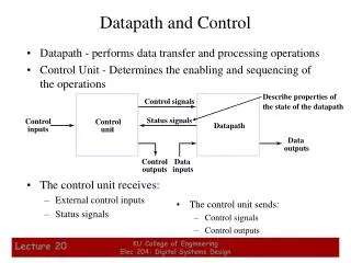
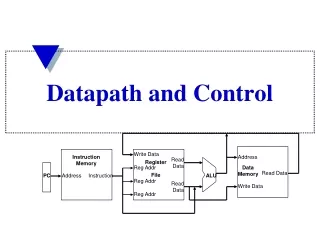
ISA Implementation • Putting everything together • A Datapath Unit • Register File A Collection of Registers • Operation Control • Decoding Instruction • Generating Control Signals to Orchestrate Hardware • Functional Units • Arithmetic Units • Logical Units • Memory Units
Data Out Data In 31 0 32-bit register R0 32-bit register R1 w 32-bit register R2 w w 32-bit register R30 32-bit register R31 w w 0 0 Reg encoding 1 Reg encoding 1 read 2 2 30 30 31 31 Register File (32 32-bit Registers) En En Write Read
Xra: X read address Yra: Y read address Xdo: X data out Ydo: Y data out Zwa: Z write address Zdi: Z data in we: write enable This register file has 2 read ports 1 write port 32 registers, each 32-bit Register File with Multiple Ports 5 5 5 Zwa Xra Yra Clock 32 Ydo RegFile 32 32 Zdi Xdo we
Adder/Subtractor Unit 32 32 A B Carry in ā/s 0: add 1: subtract AU En 32 Flags Carry out F Overflow Zero flag
Logical Unit 32 32 A B LF 4 LU En 32 F AB B A+B Ā A·B A A·B B A+B AB
LF0 LF1 AnBn 4-to-1 Mux LF2 LF3 An Bn Logical Unit Bit Slice Implementation 1 0 LF0 0 0 LF1 An·Bn 4-to-1 Mux 0 0 LF2 1 1 LF3 An Bn
Logical Unit Bit Slice Alternative Bn An 0 LF0 1 4-to-16 Decoder 6 LF1 LF2 LF3 15 Fn
B = shift amount Shift Type (ST) 00 = no shift 01 = logical shift 10 = arithmetic shift 11 = rotate Shift Direction (SD) 0 = left 1 = right Shift Unit 32 32 A B 2 ST SU En SD 32 F
32 32 Datapath Combined with Register File 5 5 5 Zwa Xra Yra Clock Ydo RegFile 32 Zdi Xdo we 32 32 A B Cin ā/s AU En 32 Flags Cout
Single Cycle Datapath 5 5 5 Zwa Xra Yra Clock 32 Ydo RegFile 32 32 Zdi Xdo we A B A B A B Cin ā/s LF ST AU LU SU En SD Flags Cout 32
Arithmetic and Logic Unit (ALU) A B A B A B Cin ā/s LF ST AU LU SU En SD Flags Cout 32 32 A B ā/s 00: AU 01: LU 10: SU 11: disable ALU 2 4 LF ALS 2 ALU ST SD I omit some input/output e.g. carry, flags etc.
32 32 Single Cycle DataPath 5 5 5 Zwa Xra Yra Clock Ydo RegFile 32 Zdi Xdo we 32 32 A B ā/s 2 4 LF ALS 2 ALU ST SD 32
DataPath with Immediate Input Sign-extended immediate Immediate Enable 5 5 5 32 1 Zwa Xra Yra Clock 32 0 Ydo RegFile 32 32 Zdi Xdo we 32 32 A B ā/s 2 4 LF ALS 2 ALU ST SD 32
st enable r/w ld enable DataPath with Memory Sign-extended immediate msel 5 5 5 32 Zwa Xra Yra 1 Clock 32 Memory Ydo 0 RegFile 32 32 Xdo Address Zdi we 32 32 A B ā/s 4 2 LF ALS ALU ST 2 SD 32 Data load $Z, ($X) store $Y, ($X)
Instruction Execution • Instruction Fetch • Given a PC address • Retrieve instruction from memory (or cache) • Instruction Decode • Instruction type, operands, etc. • Control signals • Instruction Execute • Functional unit binding • Instruction Complete • Writeback to register or memory • Can be done in single cycle or multiple cycles • Instruction complexity (CISC vs. RISC) • Pipelining
Microcode Sequencer • For a multi-cycle implementation or a CISCy ISA • Think about an x86 “string copy” instruction • An ISA instruction is translated into several microinstructions or microcode • These microinstructions • One per cycle • Harness the detailed signals inside a processor • Define low-level control signals in a given state • Microcode Sequencer • A finite state machine • Generate microinstruction sequence • Most of RISC instructions is one-to-one mapping • Could be implemented as a ROM or a PLA
Microcode Memory Datapath Control Signals Microcode Memory (ROM or PLA) Combinational Logic Needed for a multi-cycle instruction implementation State register Instruction Register
Microcode Memory Datapath Control Signals Microcode Memory (ROM or PLA) Combinational Logic Our Single-Cycle Microcode Memory • Assume all steps finish within one cycle • No state needed • Not really a microcode sequencer Instruction Register
32 Next PC gen Program Counter 32 32 32 A Simple Processor Instruction Register X 5 Y 5 Z 5 imm 16 Memory imm_en we Microcode Memory (Single-Cycle Implementation) ALS 2 Single Cycle Datapath ā/s LF 4 ST 2 SD ld_en st_en ṝ/w msel
A Simple Processor add $4, $3, $2 31 26 25 21 20 16 15 11 10 6 5 0 0 0 0 0 0 0 0 0 0 1 1 0 0 0 1 0 0 0 1 0 0 0 0 0 0 0 1 0 0 0 0 0 rs opcode rt rd shamt funct X=00011 Y=00010 Z=00100 imm=0 Memory imm_en=0 we=1 Microcode Memory ALS=00 Single Cycle Datapath ā/s=0 LF=0000 ST=00 SD=0 ld_en=0 st_en=0 ṝ/w=0 msel=0
r/w Datapath Control Signals Sign-extended immediate imm enable msel st enable 5 5 5 32 Zwa Xra Yra 1 Clock 32 Memory Ydo 0 RegFile 32 32 Xdo Address Zdi we 32 32 A B ā/s 00: AU 01: LU 10: SU 11: Disable ALU 2 4 LF ALU ALS ST 2 SD 32 Data Logical Flag 0001: AND 0011: A 0101: B 0110: XOR 0111: OR ld enable Shift Type (ST) 00: No Shift 01: Logical 10: Arithmetic 11: Rotate Shift Direction (SD) 0: Left 1: Right
Microcode Control (1) • Clear memory location 100, 104 (r0 hardwired to 0) Datapath Control Signals ALS 00: AU 01: LU 10: SU 11: Disable ALU Logical Flag (LF) 0001: AND 0011: A 0101: B 0110: XOR 0111: OR Shift Type (ST) 00: No Shift 01: Logical 10: Arithmetic 11: Rotate Shift Direction (SD) 0: Left 1: Right
Microcode Control (1) • Clear memory location 100, 104 (r0 hardwired to 0) ALS 00: AU 01: LU 10: SU 11: Disable ALU Logical Flag (LF) 0001: AND 0011: A 0101: B 0110: XOR 0111: OR Shift Type (ST) 00: No Shift 01: Logical 10: Arithmetic 11: Rotate Shift Direction (SD) 0: Left 1: Right
Microcode Control (2) • copy 4-byte data from 0xF000 to 0xA100 • clear data at 0xF000 ALS 00: AU 01: LU 10: SU 11: Disable ALU Logical Flag (LF) 0001: AND 0011: A 0101: B 0110: XOR 0111: OR Shift Type (ST) 00: No Shift 01: Logical 10: Arithmetic 11: Rotate Shift Direction (SD) 0: Left 1: Right
Microcode Control (2) • copy 4-byte data from 0xF000 to 0xA100 • clear data at 0xF000 ALS 00: AU 01: LU 10: SU 11: Disable ALU Logical Flag (LF) 0001: AND 0011: A 0101: B 0110: XOR 0111: OR Shift Type (ST) 00: No Shift 01: Logical 10: Arithmetic 11: Rotate Shift Direction (SD) 0: Left 1: Right
Microcode Control (3) • Perform r2 = 5*(r2 – 2*r3) + 3*r4 • store r2 to location stored in r10 ALS 00: AU 01: LU 10: SU 11: Disable ALU Logical Flag (LF) 0001: AND 0011: A 0101: B 0110: XOR 0111: OR Shift Type (ST) 00: No Shift 01: Logical 10: Arithmetic 11: Rotate Shift Direction (SD) 0: Left 1: Right
Microcode Control (3) • Perform r2 = 5*(r2 – 2*r3) + 3*r4 • store r2 to location stored in r10 ALS 00: AU 01: LU 10: SU 11: Disable ALU Logical Flag (LF) 0001: AND 0011: A 0101: B 0110: XOR 0111: OR Shift Type (ST) 00: No Shift 01: Logical 10: Arithmetic 11: Rotate Shift Direction (SD) 0: Left 1: Right
Instruction Fetching (PC Update) Next PC generation 32 addr Program Counter Memory 32 Instruction Register data 32x32 RegFile Datapath MicrocodeROM
Sequential Instruction Fetch 4 + 32 addr Program Counter Memory 32 Instruction Register data 32x32 RegFile Datapath Microcode ROM
Branch Support Offset (from ROM) 4 ext beq bne (if true) 0 1 mux + 32 addr Program Counter Memory 32 Instruction Register data 32x32 RegFile Datapath Microcode ROM
jr/j Branch and Jump Support rs Offset (from ROM) 4 Target addr (from ROM) ext beq bne (if true) 0 1 mux ext + 0 1 mux jr 0 1 mux j 32 addr Program Counter Memory 32 Instruction Register data 32x32 RegFile Datapath Microcode ROM