Download
1 / 16
160 likes | 292 Views
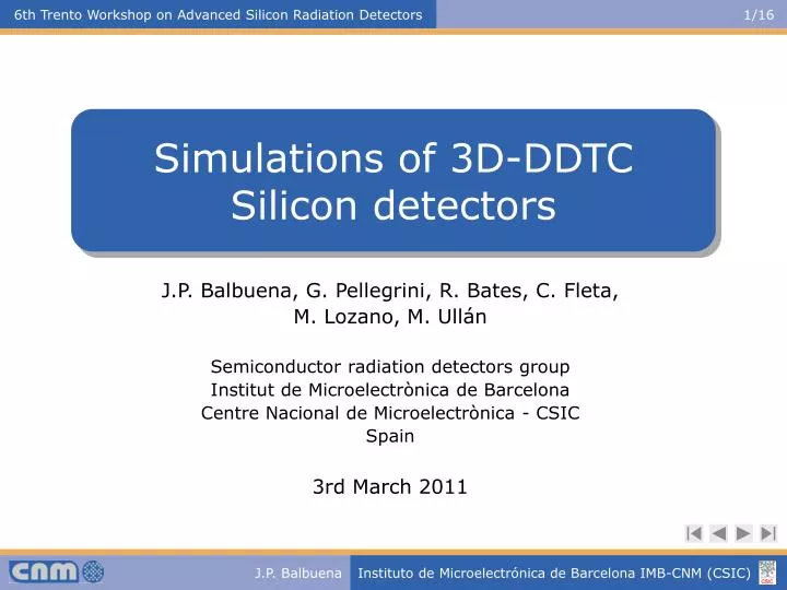
J.P. Balbuena, G. Pellegrini, R. Bates, C. Fleta, M. Lozano, M. Ullán Semiconductor radiation detectors group Institut de Microelectrònica de Barcelona Centre Nacional de Microelectrònica - CSIC Spain 3rd March 2011. Simulations of 3D-DDTC Silicon detectors.

E N D
J.P. Balbuena, G. Pellegrini, R. Bates, C. Fleta, M. Lozano, M. Ullán Semiconductor radiation detectors group Institut de Microelectrònica de Barcelona Centre Nacional de Microelectrònica - CSIC Spain 3rd March 2011 Simulations of 3D-DDTC Silicon detectors
Blocks Columns Increments Transitions Hypertext 1Motivation 2Simulation: Layout and parameters 3Simulation: Electric field 4 Simulation: Charge multiplication 5 Conclusions/Future work
Blocks Columns Increments Transitions Hypertext 1Motivation 2 Simulation: Layout and parameters 3 Simulation: Electric field 4 Simulation: Charge multiplication 5 Conclusions/Future work
3D-DDTC measurements Irradiated 3D detectors present Charge multiplication effect: Objective Develop 3D detectors with Charge multiplication effect for low Bias voltages before irradiation by changing the bulk doping concentration. • above 150V for p-type • above 260V for n-type [M. Köhler, University of Freiburg, Germany]
Blocks Columns Increments Transitions Hypertext 1 Motivation 2Simulation: Layout and parameters 3 Simulation: Electric field 4 Simulation: Charge multiplication 5 Conclusions/Future work
Geometry • - pitch: 80 µm • wafer thickness: 285 µm • column depth: 250 µm • column diameter: 10 µm Doping levels • - n+ columns: 1019 cm-3 • p+ columns: 1019 cm-3 • p-stop: 1018 cm-3 • Si/SiO2 charge: 5·1011 cm-2 P-type p+ p+ n+ p+ p+
Geometry • - pitch: 80 µm • wafer thickness: 285 µm • column depth: 250 µm • column diameter: 10 µm Doping levels • - n+ columns: 1019 cm-3 • p+ columns: 1019 cm-3 • Si/SiO2 charge: 5·1011 cm-2 N-type n+ n+ p+ n+ n+
[M. Benoit, Laboratoire de l’accélérateur linéar (LAL), Orsay, France]
Blocks Columns Increments Transitions Hypertext 1 Motivation 2 Simulation: Layout and parameters 3Simulation: Electric field 4 Simulation: Charge multiplication 5 Conclusions/Future work
Electric Field (p-type) n+ p+
Electric Field (n-type) p+ n+
Using PowerPointto Typeset Nice Presentations Blocks Columns Increments Transitions Hypertext 1 Motivation 2 Simulation: Layout and parameters 3 Simulation: Electric field 4Simulation: Charge multiplication 5 Conclusions/Future work
Charge multiplication Compromise between low full depletion voltages and high enough voltages for Charge multiplication V = 150 V for both n and p-type ρn = 100 Ω·cm ρp = 200 Ω·cm MIP 22800 electrons Charge multiplication
Charge multiplication in the irradiated 3D model Doping concentration: Neff = 7·1011 cm-3 (p-type) Fluence: Φeq = 2·1015 neq/cm2 Electric field compatible with Charge multiplication for 250V Unexpected reduction of the charge collected for 250V !! Interface charge: Qox = 5·1011 cm-2
Using PowerPointto Typeset Nice Presentations Blocks Columns Increments Transitions Hypertext 1 Motivation 2 Simulation: Layout and parameters 3 Simulation: Electric field 4 Simulation: Charge multiplication 5 Conclusions/Future work
Conclusions • Obtained charge multiplication effect in both n and p-type substrates without irradiation Future work • Complete the study on multiplication effect for different doping levels at different biasing voltages • Solve problems of charge multiplication in the irradiated 3D model.