Download
1 / 63
630 likes | 640 Views
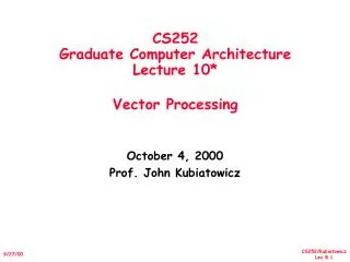
CS252 Graduate Computer Architecture Lecture 17 Caches (continued) and Memory Systems. October 29 nd , 2003 Prof. John Kubiatowicz http://www.cs.berkeley.edu/~kubitron/courses/cs252-F03. µProc 60%/yr. 1000. CPU. “Moore’s Law”. 100. Processor-Memory Performance Gap: (grows 50% / year).

E N D
CS252Graduate Computer ArchitectureLecture 17Caches (continued) and Memory Systems October 29nd, 2003 Prof. John Kubiatowicz http://www.cs.berkeley.edu/~kubitron/courses/cs252-F03
µProc 60%/yr. 1000 CPU “Moore’s Law” 100 Processor-Memory Performance Gap:(grows 50% / year) Performance 10 DRAM 7%/yr. DRAM 1 1980 1981 1982 1983 1984 1985 1986 1987 1988 1989 1990 1991 1992 1993 1994 1995 1996 1997 1998 1999 2000 Review: Who Cares About the Memory Hierarchy? • Processor Only Thus Far in Course: • CPU cost/performance, ISA, Pipelined Execution CPU-DRAM Gap • 1980: no cache in µproc; 1995 2-level cache on chip(1989 first Intel µproc with a cache on chip) “Less’ Law?”
Review: Cache performance • Miss-oriented Approach to Memory Access: • Separating out Memory component entirely • AMAT = Average Memory Access Time
Proc Proc I-Cache-1 Proc D-Cache-1 Unified Cache-1 Unified Cache-2 Unified Cache-2 Review: Harvard Architecture • Unified vs Separate I&D (Harvard) • Statistics (given in H&P): • 16KB I&D: Inst miss rate=0.64%, Data miss rate=6.47% • 32KB unified: Aggregate miss rate=1.99% • Which is better (ignore L2 cache)? • Assume 33% data ops 75% accesses from instructions (1.0/1.33) • hit time=1, miss time=50 • Note that data hit has 1 stall for unified cache (only one port) AMATHarvard=75%x(1+0.64%x50)+25%x(1+6.47%x50) = 2.05 AMATUnified=75%x(1+1.99%x50)+25%x(1+1+1.99%x50)= 2.24
Review: Reducing Misses via a“Victim Cache” • How to combine fast hit time of direct mapped yet still avoid conflict misses? • Add buffer to place data discarded from cache • Jouppi [1990]: 4-entry victim cache removed 20% to 95% of conflicts for a 4 KB direct mapped data cache • Used in Alpha, HP machines DATA TAGS One Cache line of Data Tag and Comparator One Cache line of Data Tag and Comparator One Cache line of Data Tag and Comparator One Cache line of Data Tag and Comparator To Next Lower Level In Hierarchy
Review: Improving Cache Performance 1. Reduce the miss rate, 2. Reduce the time to hit in the cache. 3. Reduce the miss penalty
0. Faster Memory 6-Transistor SRAM Cell word word (row select) 0 1 • Write: 1. Drive bit lines (bit=1, bit=0) 2.. Select row • Read: 1. Precharge bit and bit to Vdd or Vdd/2 => make sure equal! 2.. Select row 3. Cell pulls one line low 4. Sense amp on column detects difference between bit and bit 0 1 bit bit bit bit replaced with pullup to save area
1. Fast Hit times via Small and Simple Caches • Why Alpha 21164 has 8KB Instruction and 8KB data cache + 96KB second level cache? • Small data cache and clock rate • Direct Mapped, on chip
2. Fast hits by Avoiding Address Translation • Send virtual address to cache? Called Virtually Addressed Cacheor just Virtual Cache vs. Physical Cache • Every time process is switched logically must flush the cache; otherwise get false hits • Cost is time to flush + “compulsory” misses from empty cache • Dealing with aliases(sometimes called synonyms); Two different virtual addresses map to same physical address • I/O must interact with cache, so need virtual address • Solution to aliases • HW guaranteess covers index field & direct mapped, they must be unique;called page coloring • Solution to cache flush • Addprocess identifier tagthat identifies process as well as address within process: can’t get a hit if wrong process
Virtually Addressed Caches CPU CPU CPU VA VA VA VA Tags PA Tags $ TB $ TB VA PA PA L2 $ TB $ MEM PA PA MEM MEM Overlap $ access with VA translation: requires $ index to remain invariant across translation Conventional Organization Virtually Addressed Cache Translate only on miss Synonym Problem
2. Fast Cache Hits by Avoiding Translation: Process ID impact • Black is uniprocess • Light Gray is multiprocess when flush cache • Dark Gray is multiprocess when use Process ID tag • Y axis: Miss Rates up to 20% • X axis: Cache size from 2 KB to 1024 KB
2. Fast Cache Hits by Avoiding Translation: Index with Physical Portion of Address • If index is physical part of address, can start tag access in parallel with translation so that can compare to physical tag • Limits cache to page size: what if want bigger caches and uses same trick? • Higher associativity moves barrier to right • Page coloring Page Address Page Offset 31 12 11 0 Address Tag Block Offset Index
3. Fast Hit Times Via Pipelined Writes • Pipeline Tag Check and Update Cache as separate stages; current write tag check & previous write cache update • Only STORES in the pipeline; empty during a missStore r2, (r1) Check r1Add --Sub --Store r4, (r3) M[r1]<-r2& check r3 • In shade is “Delayed Write Buffer”; must be checked on reads; either complete write or read from buffer
4. Fast Writes on Misses Via Small Subblocks • If most writes are 1 word, subblock size is 1 word, & write through then always write subblock & tag immediately • Tag match and valid bit already set: Writing the block was proper, & nothing lost by setting valid bit on again. • Tag match and valid bit not set: The tag match means that this is the proper block; writing the data into the subblock makes it appropriate to turn the valid bit on. • Tag mismatch: This is a miss and will modify the data portion of the block. Since write-through cache, no harm was done; memory still has an up-to-date copy of the old value. Only the tag to the address of the write and the valid bits of the other subblock need be changed because the valid bit for this subblock has already been set • Doesn’t work with write back due to last case
Review: Improving Cache Performance 1. Reduce the miss rate, 2. Reduce the time to hit in the cache. 3. Reduce the miss penalty
0. Faster Memory • This requires a bit of discussion. • Hold a bit until we discuss memory.
1. Reducing Miss Penalty: Read Priority over Write on Miss • Write through with write buffers offer RAW conflicts with main memory reads on cache misses • If simply wait for write buffer to empty, might increase read miss penalty (old MIPS 1000 by 50% ) • Check write buffer contents before read; if no conflicts, let the memory access continue • Alternative: Write Back • Read miss replacing dirty block • Normal: Write dirty block to memory, and then do the read • Instead copy the dirty block to a write buffer, then do the read, and then do the write • CPU stall less since restarts as soon as do read
Cache Processor DRAM Write Buffer 1. Reducing Penalty: Read Priority over Write on Miss • Write Buffer is needed between the Cache and Memory • Processor: writes data into the cache and the write buffer • Memory controller: write contents of the buffer to memory • Write buffer is just a FIFO: • Typical number of entries: 4 • Works fine if:Store frequency (w.r.t. time) << 1 / DRAM write cycle • Must handle burst behavior as well!
3 8 3 8 DRAM RAS/ CAS Write DATA RAS/ CAS Read DATA Proc Processor + DRAM 8 8 3 8 3 8 Write DATA Read DATA RAS/ CAS Read DATA RAS/ CAS Write DATA RAW Hazards from Write Buffer! • Write-Buffer Issues: Could introduce RAW Hazard with memory! • Write buffer may contain only copy of valid data Reads to memory may get wrong result if we ignore write buffer • Solutions: • Simply wait for write buffer to empty before servicing reads: • Might increase read miss penalty (old MIPS 1000 by 50% ) • Check write buffer contents before read (“fully associative”); • If no conflicts, let the memory access continue • Else grab data from buffer • Can Write Buffer help with Write Back? • Read miss replacing dirty block • Copy dirty block to write buffer while starting read to memory
2. Reduce Miss Penalty: Subblock Placement • Don’t have to load full block on a miss • Have valid bitsper subblock to indicate valid • (Originally invented to reduce tag storage) Subblocks Valid Bits
3. Reduce Miss Penalty: Early Restart and Critical Word First • Don’t wait for full block to be loaded before restarting CPU • Early restart—As soon as the requested word of the block arrives, send it to the CPU and let the CPU continue execution • Critical Word First—Request the missed word first from memory and send it to the CPU as soon as it arrives; let the CPU continue execution while filling the rest of the words in the block. Also called wrapped fetch and requested word first • Generally useful only in large blocks, • Spatial locality a problem; tend to want next sequential word, so not clear if benefit by early restart block
4. Reduce Miss Penalty: Non-blocking Caches to reduce stalls on misses • Non-blocking cacheor lockup-free cacheallow data cache to continue to supply cache hits during a miss • requires F/E bits on registers or out-of-order execution • requires multi-bank memories • “hit under miss” reduces the effective miss penalty by working during miss vs. ignoring CPU requests • “hit under multiple miss” or “miss under miss” may further lower the effective miss penalty by overlapping multiple misses • Significantly increases the complexity of the cache controller as there can be multiple outstanding memory accesses • Requires multiple memory banks (otherwise cannot support) • Penium Pro allows 4 outstanding memory misses
Integer Floating Point Value of Hit Under Miss for SPEC • FP programs on average: AMAT= 0.68 -> 0.52 -> 0.34 -> 0.26 • Int programs on average: AMAT= 0.24 -> 0.20 -> 0.19 -> 0.19 • 8 KB Data Cache, Direct Mapped, 32B block, 16 cycle miss 0->1 1->2 2->64 Base “Hit under n Misses”
5. Second level cache • L2 Equations AMAT = Hit TimeL1 + Miss RateL1 x Miss PenaltyL1 Miss PenaltyL1 = Hit TimeL2 + Miss RateL2 x Miss PenaltyL2 AMAT = Hit TimeL1 + Miss RateL1x (Hit TimeL2 + Miss RateL2+ Miss PenaltyL2) • Definitions: • Local miss rate— misses in this cache divided by the total number of memory accesses to this cache (Miss rateL2) • Global miss rate—misses in this cache divided by the total number of memory accesses generated by the CPU(Miss RateL1 x Miss RateL2) • Global Miss Rate is what matters
Comparing Local and Global Miss Rates Linear • 32 KByte 1st level cache;Increasing 2nd level cache • Global miss rate close to single level cache rate provided L2 >> L1 • Don’t use local miss rate • L2 not tied to CPU clock cycle! • Cost & A.M.A.T. • Generally Fast Hit Times and fewer misses • Since hits are few, target miss reduction Cache Size Log Cache Size
Reducing Misses: Which apply to L2 Cache? • Reducing Miss Rate 1. Reduce Misses via Larger Block Size 2. Reduce Conflict Misses via Higher Associativity 3. Reducing Conflict Misses via Victim Cache 4. Reducing Conflict Misses via Pseudo-Associativity 5. Reducing Misses by HW Prefetching Instr, Data 6. Reducing Misses by SW Prefetching Data 7. Reducing Capacity/Conf. Misses by Compiler Optimizations
L2 cache block size & A.M.A.T. • 32KB L1, 8 byte path to memory
Reducing Miss Penalty Summary • Five techniques • Read priority over write on miss • Subblock placement • Early Restart and Critical Word First on miss • Non-blocking Caches (Hit under Miss, Miss under Miss) • Second Level Cache • Can be applied recursively to Multilevel Caches • Danger is that time to DRAM will grow with multiple levels in between • First attempts at L2 caches can make things worse, since increased worst case is worse
Cache Optimization Summary Technique MR MP HT Complexity Larger Block Size + – 0Higher Associativity + – 1Victim Caches + 2Pseudo-Associative Caches + 2HW Prefetching of Instr/Data + 2Compiler Controlled Prefetching + 3Compiler Reduce Misses + 0 Priority to Read Misses + 1Subblock Placement + + 1Early Restart & Critical Word 1st + 2Non-Blocking Caches + 3Second Level Caches + 2 Small & Simple Caches – + 0Avoiding Address Translation + 2Pipelining Writes + 1 miss rate miss penalty hit time
What is the Impact of What You’ve Learned About Caches? • 1960-1985: Speed = ƒ(no. operations) • 1990 • Pipelined Execution & Fast Clock Rate • Out-of-Order execution • Superscalar Instruction Issue • 1998: Speed = ƒ(non-cached memory accesses) • What does this mean for • Compilers?,Operating Systems?, Algorithms? Data Structures?
Cache Cross Cutting Issues • Superscalar CPU & Number Cache Ports must match: number memory accesses/cycle? • Speculative Execution and non-faulting option on memory/TLB • Parallel Execution vs. Cache locality • Want far separation to find independent operations vs. want reuse of data accesses to avoid misses • I/O and consistencyCaches => multiple copies of data • Consistency
Alpha 21064 • Separate Instr & Data TLB & Caches • TLBs fully associative • TLB updates in SW(“Priv Arch Libr”) • Caches 8KB direct mapped, write thru • Critical 8 bytes first • Prefetch instr. stream buffer • 2 MB L2 cache, direct mapped, WB (off-chip) • 256 bit path to main memory, 4 x 64-bit modules • Victim Buffer: to give read priority over write • 4 entry write buffer between D$ & L2$ Instr Data Write Buffer Stream Buffer Victim Buffer
Alpha Memory Performance: Miss Rates of SPEC92 I$ miss = 6% D$ miss = 32% L2 miss = 10% 8K 8K 2M I$ miss = 2% D$ miss = 13% L2 miss = 0.6% I$ miss = 1% D$ miss = 21% L2 miss = 0.3%
Alpha CPI Components • Instruction stall: branch mispredict (green); • Data cache (blue); Instruction cache (yellow); L2$ (pink) Other: compute + reg conflicts, structural conflicts
Pitfall: Predicting Cache Performance from Different Prog.(ISA, compiler, ...) • 4KB Data cache miss rate 8%,12%, or 28%? • 1KB Instr cache miss rate 0%,3%,or 10%? • Alpha vs. MIPS for 8KB Data $:17% vs. 10% • Why 2X Alpha v. MIPS? D$, Tom D$, gcc D$, esp I$, gcc I$, esp I$, Tom
Pitfall: Simulating Too Small an Address Trace I$ = 4 KB, B=16B D$ = 4 KB, B=16B L2 = 512 KB, B=128B MP = 12, 200
Main Memory Background • Performance of Main Memory: • Latency: Cache Miss Penalty • Access Time: time between request and word arrives • Cycle Time: time between requests • Bandwidth: I/O & Large Block Miss Penalty (L2) • Main Memory is DRAM: Dynamic Random Access Memory • Dynamic since needs to be refreshed periodically (8 ms, 1% time) • Addresses divided into 2 halves (Memory as a 2D matrix): • RAS or Row Access Strobe • CAS or Column Access Strobe • Cache uses SRAM: Static Random Access Memory • No refresh (6 transistors/bit vs. 1 transistorSize: DRAM/SRAM 4-8, Cost/Cycle time: SRAM/DRAM 8-16
Main Memory Deep Background • “Out-of-Core”, “In-Core,” “Core Dump”? • “Core memory”? • Non-volatile, magnetic • Lost to 4 Kbit DRAM (today using 64Kbit DRAM) • Access time 750 ns, cycle time 1500-3000 ns
1-Transistor Memory Cell (DRAM) row select • Write: • 1. Drive bit line • 2.. Select row • Read: • 1. Precharge bit line to Vdd/2 • 2.. Select row • 3. Cell and bit line share charges • Very small voltage changes on the bit line • 4. Sense (fancy sense amp) • Can detect changes of ~1 million electrons • 5. Write: restore the value • Refresh • 1. Just do a dummy read to every cell. bit
DRAM Capacitors: more capacitance in a small area • Trench capacitors: • Logic ABOVE capacitor • Gain in surface area of capacitor • Better Scaling properties • Better Planarization • Stacked capacitors • Logic BELOW capacitor • Gain in surface area of capacitor • 2-dim cross-section quite small
Classical DRAM Organization (square) bit (data) lines r o w d e c o d e r Each intersection represents a 1-T DRAM Cell • Row and Column Address together: • Select 1 bit a time RAM Cell Array word (row) select Column Selector & I/O Circuits row address Column Address data
RAS_L CAS_L WE_L OE_L A 256K x 8 DRAM D 9 8 RAS_L DRAM Read Timing • Every DRAM access begins at: • The assertion of the RAS_L • 2 ways to read: early or late v. CAS DRAM Read Cycle Time CAS_L A Row Address Col Address Junk Row Address Col Address Junk WE_L OE_L D High Z Junk Data Out High Z Data Out Read Access Time Output Enable Delay Early Read Cycle: OE_L asserted before CAS_L Late Read Cycle: OE_L asserted after CAS_L
4 Key DRAM Timing Parameters • tRAC: minimum time from RAS line falling to the valid data output. • Quoted as the speed of a DRAM when buy • A typical 4Mb DRAM tRAC = 60 ns • Speed of DRAM since on purchase sheet? • tRC: minimum time from the start of one row access to the start of the next. • tRC = 110 ns for a 4Mbit DRAM with a tRAC of 60 ns • tCAC: minimum time from CAS line falling to valid data output. • 15 ns for a 4Mbit DRAM with a tRAC of 60 ns • tPC: minimum time from the start of one column access to the start of the next. • 35 ns for a 4Mbit DRAM with a tRAC of 60 ns
Main Memory Performance Cycle Time Access Time Time • DRAM (Read/Write) Cycle Time >> DRAM (Read/Write) Access Time • 2:1; why? • DRAM (Read/Write) Cycle Time : • How frequent can you initiate an access? • Analogy: A little kid can only ask his father for money on Saturday • DRAM (Read/Write) Access Time: • How quickly will you get what you want once you initiate an access? • Analogy: As soon as he asks, his father will give him the money • DRAM Bandwidth Limitation analogy: • What happens if he runs out of money on Wednesday?
Increasing Bandwidth - Interleaving Access Pattern without Interleaving: CPU Memory D1 available Start Access for D1 Start Access for D2 Memory Bank 0 Access Pattern with 4-way Interleaving: Memory Bank 1 CPU Memory Bank 2 Memory Bank 3 Access Bank 1 Access Bank 0 Access Bank 2 Access Bank 3 We can Access Bank 0 again
Main Memory Performance • Simple: • CPU, Cache, Bus, Memory same width (32 bits) • Wide: • CPU/Mux 1 word; Mux/Cache, Bus, Memory N words (Alpha: 64 bits & 256 bits) • Interleaved: • CPU, Cache, Bus 1 word: Memory N Modules(4 Modules); example is word interleaved
address address address address 0 1 4 5 2 3 9 8 6 7 13 12 10 11 14 15 Bank 1 Bank 0 Bank 2 Bank 3 Main Memory Performance • Timing model • 1 to send address, • 4 for access time, 10 cycle time, 1 to send data • Cache Block is 4 words • Simple M.P. = 4 x (1+10+1) = 48 • Wide M.P. = 1 + 10 + 1 = 12 • Interleaved M.P. = 1+10+1 + 3 =15
Avoiding Bank Conflicts • Lots of banks int x[256][512]; for (j = 0; j < 512; j = j+1) for (i = 0; i < 256; i = i+1) x[i][j] = 2 * x[i][j]; • Even with 128 banks, since 512 is multiple of 128, conflict on word accesses • SW: loop interchange or declaring array not power of 2 (“array padding”) • HW: Prime number of banks • bank number = address mod number of banks • address within bank = address / number of words in bank • modulo & divide per memory access with prime no. banks? • address within bank = address mod number words in bank • bank number? easy if 2N words per bank
Fast Bank Number • Chinese Remainder TheoremAs long as two sets of integers ai and bi follow these rules and that ai and aj are co-prime if i j, then the integer x has only one solution (unambiguous mapping): • bank number = b0, number of banks = a0 (= 3 in example) • address within bank = b1, number of words in bank = a1 (= 8 in example) • N word address 0 to N-1, prime no. banks, words power of 2 Seq. Interleaved Modulo Interleaved Bank Number: 0 1 2 0 1 2Address within Bank: 0 0 1 2 0 16 8 1 3 4 5 9 1 172 6 7 8 18 10 2 3 9 10 11 3 19 11 4 12 13 14 12 4 20 5 15 16 17 21 13 5 6 18 19 20 6 22 14 7 21 22 23 15 7 23
Independent Memory Banks • Memory banks for independent accesses vs. faster sequential accesses • Multiprocessor • I/O • CPU with Hit under n Misses, Non-blocking Cache • Superbank: all memory active on one block transfer (or Bank) • Bank: portion within a superbank that is word interleaved (or Subbank) … Superbank Bank Superbank Offset Superbank Number Bank Offset Bank Number