Download
1 / 27
270 likes | 275 Views
Learn the basics of PCB design, including schematic creation, component placement, trace routing, and more. Understand the terminology and guidelines for creating a high-quality printed circuit board.

E N D
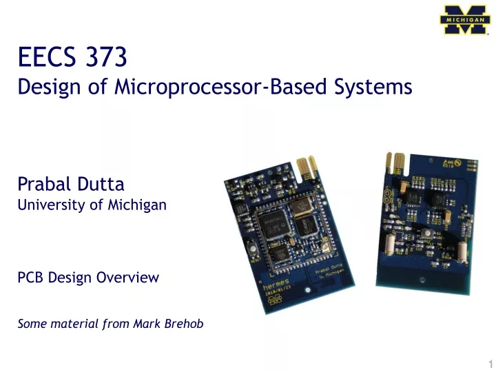
EECS 373 Design of Microprocessor-Based Systems Prabal Dutta University of Michigan PCB Design Overview Some material from Mark Brehob
So you want to make a PCB?! • A PCB is just a set of wires that connect components. • But there are some issues • The wires have restricted dimensionality • The wires are very thin • So high resistance (as conductors go) • The board needs to include holes (or pads) for the devices. • You can’t easily change things once you build it. http://www.linkwitzlab.com/Pluto/supplies-subw.htm, http://www.musicfromouterspace.com/analogsynth/SINGLEBUSSKEYBOARD2007/SINGLEBUSSKEYBOARD2007.php
Basic Terminology • The wires you are laying out are called “traces” or “tracks” • Inside of a given “layer” tracks which cross are electrically connected. • If you have traces on both sides of the board, you are said to have to layers. • Through-hole:Having pins designed to be inserted into holes and soldered to pads on a printed board. • Contrast with surface mount where device goes on top.
Starting with the end in mind: a printed circuit board Copper (pads & traces) Silkscreen (white) Soldermask (green) Bottom side Top side Drill files (size & x-y coords)
Step 1: Schematic • The first thing you want is something that looks like a textbook circuit diagram. It just shows the devices and how they are connected. • Sometimes you will worry about pinouts here (say when working with a microprocessor maybe) • But usually you don’t • No notion of layout belongs here!
Why a schematic? • In general it is drawn to be readable. • This is probably what your sketch on paper would look like. • You can find and fix bugs more easily here than the PCB layout.
Once you know what it is you want to build, you need to figure out how to lay it out on the board. You need to know how big each piece is, and where the holes need to be placed. Each device has a pattern which shows exactly that. You will occasionally need to create a pattern. Patterns
Placement • You need to place the patterns on the board. • You need to not overlap them so that the components can actually fit on the board. • You want to leave room for the traces to connect everything. • This is very much an art form. • In fact you will find people who rant about “sloppy” or “unprofessional” placements. • Some tools will do this for you. No one seems to like them. (Actually, some are not that bad)
Routing • A route (or net) is a connection between devices. • It may consist of multiple traces • There are design rules which include: • Minimum trace width • Minimum spacing between traces and holes • Minimum spacing between holes and holes. • These rules will vary by manufacturer. • Even better, units will vary by manufacturer!
Issues of measure • PCB land uses some interesting terminology. • A “thou” is a thousandth of an inch. • A “mm” is a millimeter • A “mil” is a thousandth of an inch. • Thou is generally preferred over mill to avoid confusion, but most tools/vendors use mil.
Trace width • In general most PCB manufacturers seem to have trace-width minimums of 6-10 thous. • Most are willing to go smaller for a price. • A rule of thumb is to use a 50 thou minimum for power/ground and 15-25 for everything else. • This is to drop the resistance of the traces. • In general you are worried about heat dissipation • There are lots of guidelines for width/power but in general you are looking at: • A 10cm trace needs to be 10 thou wide if it will carry 1 amp. • 5 amps at 10cm would require 110 thou.
Trace width continued • The problem with wide traces is that they are hard to route. • In particular you might wish to go between pins of a device. • One solution is to be wide normally and “neck down” when you have to. • This is more reasonable than you think. • Think resistors in series.
A rat’s nest shows the placement of the devices and the connections but not the routing Rat’s nest.
You can use an autorouter to route your traces Some people hate these as the design will be “ugly” Saves a lot of time. Oddly, not as good as a person can do. But much faster. Routing for real
Vias • Sometimes you need to connect two traces on two different layers. • To do this we use a via. • It is just a a plated through hole • Generally smaller than a through hole for a part.
Clearances • Again there will be space between the traces, plated holes and each other. • You need to meet the requirement of the manufacturer. • 15 thou is a good idea • Often you can drop to 6 or 10. • For high-power systems there are rules about this stuff.
Other things: • Silkscreen • Use this to label parts to insert, directions parts go, names user might want (on/off for example) • Solder mask or solder resist • a lacquer-like layer of polymer that provides a permanent protective coating for the copper traces of a (PCB) and prevents solder from bridging between conductors, thereby preventing short circuits. • Solder mask is traditionally green but is now available in many colors.
Sources • http://alternatezone.com/electronics/files/PCBDesignTutorialRevA.pdf • Very nice tutorial/overview • Seems to have strong viewpoint • http://www.goldengategraphics.com/pcgloss.htm • Some definitions taken verbatim. • Wikipedia • And others where noted
Questions? Comments? Discussion?