Download
1 / 15
150 likes | 287 Views
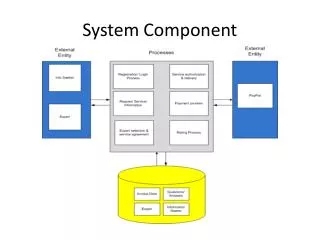
Adding the TSE component to BANSMOM system and Software Development. m 5151117 Yumiko Kimezawa. Outline. Previous Work Implementing a Triple-Speed Ethernet (TSE) component (Hardware) Current Work Adding the TSE component to BANSMOM system Software Development (unfinished) Future Work.

E N D
RPS Adding the TSE component to BANSMOM system and Software Development m5151117 Yumiko Kimezawa
Outline RPS • Previous Work • Implementing a Triple-Speed Ethernet (TSE) component (Hardware) • Current Work • Adding the TSE component to BANSMOM system • Software Development (unfinished) • Future Work
Triple-Speed Ethernet (TSE) part RPS • Components • Triple-Speed Ethernet • TX SDGMA • RX SGDMA dispensable User Interface Host PC Stratix III Transfer ? Receive
Optimized HW RPS • Block diagram of optimized hardware : Data flow : Control signal 1: Signal Reading Ethernet PHY JTAG UART LED Graphic LCD FPGA Graphic LCD Controller PPD CPU PPD CPU Memory LED Controller External Memory Raw ECG data TSE MAC Avalon Bus TX SGDMA Shared Memory Timer Master CPU Master CPU Memory FIR Filter Timer PPD Module Ethernet Master Module
Optimized HW RPS • Block diagram of optimized hardware 2: Filtering : Data flow : Control signal Ethernet PHY JTAG UART LED Graphic LCD FPGA Graphic LCD Controller PPD CPU PPD CPU Memory LED Controller External Memory Raw ECG data TSE MAC Avalon Bus TX SGDMA Shared Memory Timer Master CPU Master CPU Memory FIR Filter Timer PPD Module Ethernet Master Module
Optimized HW RPS • Block diagram of optimized hardware : Data flow : Control signal 3: Processing Ethernet PHY JTAG UART LED Graphic LCD FPGA Graphic LCD Controller PPD CPU PPD CPU Memory LED Controller External Memory Raw ECG data TSE MAC Avalon Bus TX SGDMA Shared Memory Timer Master CPU Master CPU Memory FIR Filter Timer PPD Module Ethernet Master Module
Optimized HW RPS 4: Display & Transferring data • Block diagram of optimized hardware : Data flow : Control signal Ethernet PHY JTAG UART LED Graphic LCD FPGA Graphic LCD Controller PPD CPU PPD CPU Memory LED Controller External Memory Raw ECG data TSE MAC Avalon Bus TX SGDMA Shared Memory Timer Master CPU Master CPU Memory FIR Filter Timer PPD Module Ethernet Master Module
Software Development RPS • Creating a NicheStack TCP/IP stack and MicroC-OS/II • Now, I am investigating
Software Architecture Model RPS • The onion diagram shows the architectural layers of a Nios II MicroC/OS-II software application Application Application-specific system initialization NicheStack TCP/IP Stack software component Software Micro C/OS - II HAL API Software device driver Nios II Processor system hardware Hardware
Future Work RPS • Investigating NicheStack TCP/IP stack and MicroC-OS/II to get data from shared memory and send it to the host PC
Optimized HW (Proposal) RPS : Data flow : Control signal Ethernet PHY JTAG UART LED Graphic LCD FPGA Graphic LCD Controller PPD CPU PPD CPU Memory LED Controller External Memory Raw ECG data TSE MAC Avalon Bus TX SGDMA Shared Memory Timer Master CPU Master CPU Memory FIR Filter Timer PPD Module Ethernet Master Module
Optimized HW (Proposal) RPS : Data flow : Control signal Ethernet PHY JTAG UART LED Graphic LCD FPGA Graphic LCD Controller PPD CPU PPD CPU Memory LED Controller External Memory Raw ECG data TSE MAC Avalon Bus TX SGDMA Shared Memory Timer Master CPU Master CPU Memory FIR Filter Timer PPD Module Ethernet Master Module
Optimized HW (Proposal) RPS : Data flow : Control signal Ethernet PHY JTAG UART LED Graphic LCD FPGA Graphic LCD Controller PPD CPU PPD CPU Memory LED Controller External Memory Raw ECG data TSE MAC Avalon Bus TX SGDMA Shared Memory Timer Master CPU Master CPU Memory FIR Filter Timer PPD Module Ethernet Master Module
Optimized HW (Proposal) RPS • Block diagram of optimized hardware : Data flow : Control signal Ethernet PHY JTAG UART LED Graphic LCD FPGA Graphic LCD Controller PPD CPU PPD CPU Memory LED Controller External Memory Raw ECG data TSE MAC Avalon Bus TX SGDMA Shared Memory Timer Master CPU Master CPU Memory FIR Filter Timer PPD Module Ethernet Master Module