Download
1 / 18
180 likes | 321 Views
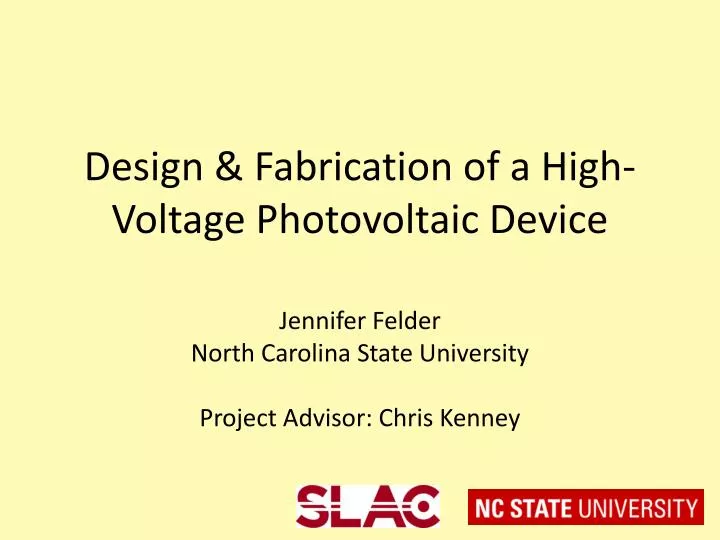
Design & Fabrication of a High-Voltage Photovoltaic Device. Jennifer Felder North Carolina State University Project Advisor: Chris Kenney. Outline. Brief Review Motivation Unique Features of Design (Mask) Design Simulation Fabrication Conclusion. A Brief Review. Photoelectric Effect

E N D
Design & Fabrication of a High-Voltage Photovoltaic Device Jennifer Felder North Carolina State University Project Advisor: Chris Kenney
Outline • Brief Review • Motivation • Unique Features of Design • (Mask) Design • Simulation • Fabrication • Conclusion
A Brief Review • Photoelectric Effect • Photovoltaic (PV) Effect/Devices Image courtesy of: http://amazingdata.com/mediadata8/Image/amazing_fun_science_technology_20090729124730244.jpg
Project Motivation • High-Voltage PV • EXO Experiment Power Source • Unique Features of Device • Wavelength • Temperature • Float-zone Si wafers • Impurities • Cost
Wavelength Matching • Band gap & efficiency • Band gap of Si = 1.12 eV • λ=hc/E 1.12 eV~ 1100 nm • Solar cells?
Temperature & Efficiency • η drops 0.1% per °C above 25°C • Ex: If it were 105°F (40.5°C) -1.55% • Liquid Xe • Solar cells?
Preliminary Calculations 1. Known Parameters 2. Modeling Equations 3. Calculated Parameters
Mask Design: PV Device • Series Connections • Various Voltages (50-2000 V) • From Calculations:
3 Basic Cell Designs Simulated SOI Layer P Diffusion N Diffusion
Optimized Cell Design • N-type diffusion area • Constraints on area size
Built-in Potential • High built-in potential fewer number cells • Φj≈ 0.97 V (± 0.01 V between designs) • Not a deciding factor
SRH Recombination • Low recombination high photovoltage generation
Fabrication • Stanford Nanofabrication Facility (SNF) • Wet oxidation process • Remove organic materials • Remove metal ions • Oxidation • Other steps to be finished in future work…
Conclusions • Feasibility/Proof of Concept Test • Significant Impact • Experiments (EXO) • Noise • SLAC • Extended to other PV/solar cell technology, many others!
Acknowledgments • Chris Kenney • Jasmine Hasi • Astrid Tomada • Julie Segal • DOE • SLAC & SNF Staff
Questions, Comments, Concerns? Feel free to e-mail me at jkfelder@ncsu.edu