Download
1 / 18
180 likes | 276 Views
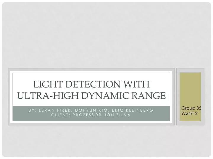
Light Detection with Ultra-High Dynamic Range. Group 35 9/24/12. By: Leran Firer, Dohyun Kim, Eric Kleinberg Client: Professor Jon Silva. Client Request. Need: Dr. Silva requested to design a light detection system with high signal to noise ratio.

E N D
Light Detection with Ultra-High Dynamic Range Group 35 9/24/12 By: Leran Firer, Dohyun Kim, Eric Kleinberg Client: Professor Jon Silva
Client Request • Need: Dr. Silva requested to design a light detection system with high signal to noise ratio. Figure 1: A Typical Fluorescence Microscope System
Background • Fluorescence Microscopy is a recently developed technique that allows for the observation of conformational/functional changes in proteins. Figure 2: Example of a Protein Viewable by Fluorescence Microscopy
Scope • Must accurately amplify/filter signal 0.1% in magnitude relative to background (pA). • Must focus light to the diffraction limit onto the PIN diode of electrical system. • Must keep photo diode cool to reduce noise. Figure 3: The Three Main Parts of the Project
Specifications Table 1: Specifications
Team Organization • Dohyun: PIN Diode Selection and Electrical System Design • PIN Diode • Integrating Amplifier/ Biasing • Bessel Filter • Current/Voltage Translator • Leran: Fluorescence Focusing System Design • Lens Selection • Mounting Design • Eric: Cooling System Design • Peltier Cooler
Existing Solutions Figure 4: Photomax 200 • Photomax 200 by Dagan Corporation. • Cost: $10,850-13,900 depending on configuration. • 4 Poles Bessel Filter • Up to 300 volt diode bias voltage • 2 Stages Peltier Cooled • Band Pass of Blue and Green Lights • Digitally filtered.
Patent and Literature • Chris S. Gandhi, The Voltage-Clamp FluorometryTechnique, Methods Mol Biol. 2009 ;491 :213-31 18998096 • A.J. Horne and D. Fedida, Use of Voltage Clamp Fluorimetryin Understanding Potassium Channel Gating: A Review of Shaker Fluorescence Data,Can J PhysiolPharmacol. 2009 Jun;87(6):411-8 • Thomas Kugelstadt, Active Filter Design Techniques, Literature Number SLOA088, Excerpted from Op Amps for Everyone, Literature Number: SLOD006A
Patent and Literature US5054896: Continuously focusable microscope incorporating an afocalvariator optical system Figure 5: AfocalVariator Optical System
Preliminary Analysis Table 2: Pugh Chart for PIN Diode Selection * Decision yet to be made
Preliminary Analysis Filter Design and Selection • Bandpass Filter: 5-10 kHz-Butterworth-Bessel-Schenk • Bessel Filter: preserves the wave shape of filtered signals in the passband. Figure 6: Bessel Filter Schematic
Preliminary Analysis Actual Calculations • Center Frequency FM= 7.5KHz • Bandwidth B= 5kHz • Q= FM/B = 1.5 • Center Gain Km = 1 (absolute value); Unity gain filter • From the Coefficient of the 4th order Filter Tablea1 = 1.3617b1 = 0.6180 α = 1.2711 (at Q = 1.5)Fm1 = FM/ α = 5900.4 →Fm2 = FM* α = 9533.3C = 10 nF
Preliminary Analysis Figure 7: 4th Order Bessel Bandpass Filter Designed with Commercially Available Resistors and Capacitors
Preliminary Analysis Table 3: Lens Types Singlet lenses are simple and easy to use, but a multi element lens system is favorable performance wise to avoid aberrations.
Preliminary Analysis Figure 8: Spherical (left) and Chromatic (right) Aberrations Diffraction Spot Size Equation 1: d= 2.44*λ*f d - diameter f - focal length λ - wavelength Figure 9: Achromatic Doublet Focusing
Preliminary Analysis Table 4: An Overview of Thermal Interfaces
Design Schedule Table 5: Schedule
Picture Sources • Slide 2 Picture: The Voltage-Clamp FluorometryTechnique ,Chris S. Gandhi and Riccardo Olcese • Slide 3 Picture: BME 301B, Dr. Cui’s Ion Channels lecture • Slide 4 Pictures: Lens from Thor Labs, PIN Diode from http://www.shinebon.com/images/products/2011122165018597w1000h1000ushinebon/high-power-pin-diode.jpg, PeltierCooler from http://www.dansdata.com/images/pelt/peltier400.jpg • Slide 7 Picture: Dagan Corporation, http://www.dagan.com/photomax-200.htm • Slide 10 Pictrure: US5054896, http://www.google.com/patents?id=g3sjAAAAEBAJ&pg=PA2&dq=optical+focusing+system+achromatic+doublet+lens&source=gbs_selected_pages&cad=4#v=onepage&q&f=false • Slide 15 Figure 8 and 9: Lens, lens system, and optical aberrations http://www.cartage.org.lb/en/themes/sciences/physics/optics/Optical/Lens/Lens.htm