Download
1 / 18
950 likes | 3.5k Views
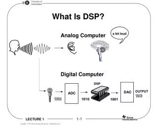
Analog to Digital Converters (ADCs) & Digital to Analog Converters (DACs). Analog to Digital Conversion (ADC). Analog to Digital Conversion is the process by which analog signals are converted to their digitized forms. ADC occurs via three steps: - Sampling. - Quantization.

E N D
Analog to Digital Converters(ADCs)& Digital to Analog Converters (DACs)
Analog to Digital Conversion (ADC) • Analog to Digital Conversion is the process by which analog signals are converted to their digitized forms. • ADC occurs via three steps: - Sampling. - Quantization. - Encoding.
The idea of Sampling • The analog signal is sampled at regular intervals of time. • The sampling rate must be at least twice the highest frequency of the signal ( Nyquist Criterion).
Quantization • Quantization is defined as the process of converting the continuous sample amplitude into a discrete amplitude. Thus by then, the signal will be discrete in both; time and amplitude.
Quantization Error • The difference between the actual analog value and quantized digital value.
Encoding • Encoding is the process which assigns ones and zeros (stream of bits) for every quantization level. • The number of bits assigned for each level (n) depends on the levels’ number (L) ; such that L= 2^n.
Ideal ADC Q= Δ=quantization step = full scale / levels’ number. In an ideal analog-to-digital converter, the quantization error is uniformly distributed between –Δ/2 and Δ/2. The resolution of the ADC is the smallest detectable change in voltage.
Types Of ADCs • There are many types of ADCs such as: • Direct Conversion ADC. • Successive Approximation Register (SAR) ADC. • Integrating ADCs: Single slope, dual slope, and ramp ADC. • Sigma-Delta ADC (over sampled ADC). • ADC0804 Analog to Digital Converter. In our experiment ADC0804 , and the SAR ADC are explained.
ADC0804 Analog to Digital Converter • ADC0804 is a 20-pin IC with an 8-bit resolution. • The analog input voltage range is from 0 V to 5 V, with 15 mW power consumption and 100 us conversion time .
SAR ADC • It is one of the popular ADCs for 8-16 bits. • It has moderate conversion speeds ; the conversion time is around 1 Us. • It doesn’t consume a lot of power and its cost is low in comparison with the other types. • On the other hand, it requires a sample and hold circuit and it can have missing output codes.
Example: Vref=5V, Vs=3.127V, 4-bits.(b1b2b3b4) Set b1=1 all b2b3b4=000 >> 1000 Vdac=8*5/(2^4)=2.5V (Vdac=2.5)>(Vs=3.127) No!! b1=1 2. Set b2=1 all b3b4=00 >> 1100 Vdac=12*5/(2^4)=3.75V (Vdac=3.75)>(Vs=3.127) Yes b2=0 3. Set b3=1 b4=0 >> 1010 Vdac=10*5/(2^4)=3.125V (Vdac=3.125)>(Vs=3.127) No!! b3=1 4. Set b4=1 >>1011 Vdac=11*5/(2^4)=3.4375V (Vdac=3.4375)>(Vs=3.127) Yes b4=0 Final Result=1010
Digital To Analog Conversion ( DAC) • Digital to analog converter (DAC) is the device which converts digital signals to analog ones. • Most of the DACs consist of a network of resistors and analog switches. • The switches control the currents or voltages that are derived from a particular reference voltage and provide analog output current.
Types Of DACs • There are many types of DACs such as: • Weighted resistor DAC. • R-2R DAC. • General purpose DAC ( DAC 0800). • Frequency to voltage converter. • Pulse width modulation. In our experiment, R-2R DAC and the general purpose DAC are explained.
R-2R DAC • The Block diagram of R-2R DAC is as shown below: • The analog output is given by the following equation: • The highest resistance value is only 2R and thus requires an area inside the IC less 8 times than that of the weighted resistor DAC which highest resistance is 16R.
The DAC analog output is represented by current. This current is the ratio of the input code to the full scale voltage (Vref) as given in the following equation: • So, an operational amplifier is needed to convert the current to voltage level.
The General Purpose ( DAC 0800) • The block diagram of DAC 0800 is as shown below: • It’s clear that it’s a 8-bit DAC with 16 pins IC. • The conversion time is around 100ns.
Bipolar/ Unipolar DACs • For unipolar DACs, the output voltage is given by: • For bipolar DACs, the output voltage is given by: