Download
1 / 158
1.58k likes | 1.71k Views
Experiment 3 Lab 6 Outline Presentation Digital product development overview Component selection for a new chip Xilinx component usage Using A Brief Look at Semiconductor Technology Moore’s Law , smaller transistors , their implications and potential issues

E N D
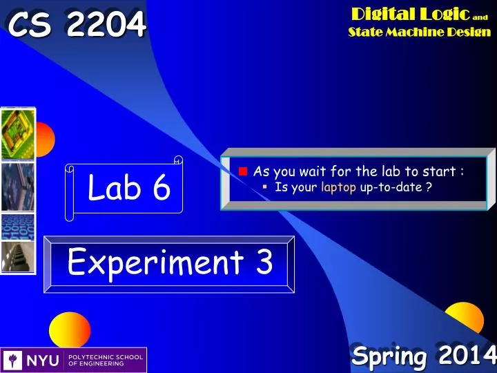
Experiment 3 Lab 6 Outline • Presentation • Digital product development overview • Component selection for a new chip • Xilinx component usage • Using A Brief Look at Semiconductor Technology • Moore’s Law, smaller transistors, their implications and potential issues • Analysis of the term project • Analysis of Block 6 of the term project (using Term Project pages 38-48) • Implementing a machine player • A machine playing strategy • Individual work • Experiment 3 • Develop the Rightmost Zero Display circuit of the Ppm term project • Develop a new machine player that uses the Rightmost Zero Display circuit • New handouts • Digital Product Development CS 2204 Spring 2014
Presentation • Developing a Digital Product • CS2204 sets out to develop a prototype • A prototype chip • A prototype PCB • If everything goes well and the product is not obsolete, it is mass produced • Mass produce the prototype chip • Whoever wants to use the chip must develop a new PCB • Mass produce the prototype PCB CS 2204 Spring 2014
Developing a new chip TEST : applying input combinations, test vectors, and simulating 1)Development Cycle on Computers During testing If you see MODIFYING hardware to optimize it is possible, do that after you correct logic and timing errors. Then, test again to see if your minimization has logic/timing errors DESIGN TEST MODIFY Major error :Redesign Major error :Redesign or terminate the project due to TTM Mount : FPGAs are mounted on bread/boards, wired and programmed 2)Development Cycle with FPGA chips Test : apply test vectors to FPGAs Mount Test Modify Modify : either FPGA mounting/wiring is changed or a simple design change is made on computers, simulated, then FPGAs are programmed and tested Major error : Redesign or terminate the project due to TTM 3)Development Cycle on prototype chip Fabricate chip by sending a GDSII file to a fabrication facility : tape out Fabricate Test Apply test vectors to the chip CS 2204 Spring 2014
Developing a new PCB TEST : Simulating by applying input combinations, test vectors, may not be possible. It may be coarse grain simulation 1) Development Cycle on Computers During testing if you see MODIFYING hardware to optimize it is possible, do that after you correct logic and timing errors. Then, test again to see if your minimization has logic/timing errors DESIGN TEST MODIFY Major error : Redesign Major error : Redesign or terminate the project due to TTM Mount : Chips are mounted on bread/boards and wired 2) Dev. Cycle with off-the-shelf chips Mount Test Modify Test : apply test vectors to the chips Modify : chip mounting/wiring is changed and tested or a simple design change is made on computers, simulated, then chip mounting/wiring is changed and tested Major error : Redesign or terminate the project due to TTM 3) Dev. Cycle on prototype PCB Fabricate PCB at a fabrication facility, mount chips and other components Fabricate Test Modify Apply test vectors to the PCB Modify means chip mounting/wiring is changed and tested CS 2204 Spring 2014
CS 2204 Spring 2014 • Developing a Digital Product • In the lab we use the FPGA chip • In the lab, we practice how to develop a new chip • In the classroom we discuss both • How to develop a new chip • How to develop a new PCB
CS2204Lab New Chip Development Steps • Development Cycle on Computers • As described above • Development Cycle with FPGA chips • Mount : we will not mount FPGAs nor wire them • We will just program FPGAs • Test • Applytest vectors by using switches and push buttons • Observe the 7-segment displays and LED lights • Modify • A simple schematic design change is made on the computer, simulated, then the FPGA is programmed and tested CS 2204 Spring 2014
What are these components ? Today’s work • Xilinx Project Development Steps • Develop the schematic • Design the schematic • Design blocks, (sub)blocks • Place the components and wires • Do a schematic check • Test the schematic via functional simulations • Do a Xilinx IMPLEMENTATION • It maps the components to the CLBs of the chip • Do timing simulations to test the schematic • It generates the bit file • Download the bit file to the FPGA and test the design on the board • It programs the chip Development Cycle on Computers Development Cycle with FPGA chips CS 2204 Spring 2014
CS 2204 Spring 2014 • Developing a digital product • A new chip • Which gates & FFs and how many is determined by • The application (major operations) • Available chips of the technology chosen • Besides speed, cost, power, etc. : design goals • We will try to use high density components (MUXes, decoders, adders, comparators, encoders, deMUXes, registers, counters, shift registers) as much as possible • We will try not to use low-density components (gates and flip-flops) • We will work on chips design in the lab and classroom • Labs, lectures, homework assignments, the term project and exams
Use these as much as possible Generic components Lectures, homework, exams Xilinx components Labs Flip-flops Gates Popular digital circuits Gates Flip-flops Popular digital circuits ADDer Comparator Multiplexer DeMux Decoder Encoder ALU Counter Register … ADDer Comparator Multiplexer DeMux Decoder Encoder ALU Counter Register … AND OR NOT NAND NOR … D JK T SR … AND OR NOT NAND NOR … D T JK High-density components To save time, space, power. weight,… CS 2204 Spring 2014 • CS2204 Components • Available components for a new chip
1 generic inverter 2 generic 2-input AND gates 1 generic 2-input OR gate a NOT AND b Total : 4 generic components used OR a AND c y(a, b, c) =a.b + a.c Which generic components ? CS 2204 Spring 2014 • Implementing a Combinational Circuit on a NewChip • By using generic components that are AND, OR, NOT,… • The 2-to-1 MUX
a NOT AND b OR a AND c y(a, b, c) =a.b + a.c Use a generic 2-to-1 MUX already designed Do not design your own 2-to-1 MUX CS 2204 Spring 2014 • Implementing a Combinational Circuit on a New Chip • By using generic components that are AND, OR, NOT • The 2-to-1 MUX
Sel a 2-to-1 MUX 0 y b 1 generic 2-to-1 MUX 1 c Total : 1 generic component used a NOT AND b OR a AND c y(a, b, c) =a.b + a.c Which generic components ? CS 2204 Spring 2014 • Implementing a Combinational Circuit on a New Chip • The 2-to-1 MUX • Use a generic 2-to-1 MUX already designed
2 generic inverters 5 generic 2-input AND gates 1 generic 5-input OR gate Total : 8 generic components used 2-bit Unsigned Binary Comparator From Handout 3 Which generic components ? Output z = 1 if (a,b) > (c, d) CS 2204 Spring 2014 • Implementing a Combinational Circuit on a NewChip • By using generic components that are AND, OR, NOT,…
Implementing a Combinational Circuit on a New Chip By using generic components that are AND, OR, NOT,… • 2-bit Unsigned Binary Comparator Use a generic comparator already designed You need an extraNOT gate besides the comparator Do not design your own Comparator CS 2204 Spring 2014
1 generic 2-bit Unsigned Comparator 1 generic NOT gate Total : 2 generic components used Which generic components ? a b c d A1 A0 B1 B0 2-bit Unsigned Binary Comparator AGTB AEQB ALTB Output z = 1 if (a,b) > (c, d) z CS 2204 Spring 2014 • Implementing a Combinational Circuit on a New Chip • 2-bit Unsigned Binary Comparator • By using a generic comparator already designed
Lab design Use Xilinx macros as much as possible Try not to use these components Xilinx components Labs Generic components Lectures, homework, exams Gates Flip-flops Popular digital circuits Gates Flip-flops Popular digital circuits ADDer Comparator Multiplexer DeMux Decoder Encoder ALU Counter Register … D T JK AND OR NOT NAND NOR … AND OR NOT NAND NOR … D JK T SR ADDer Comparator Multiplexer DeMux Decoder Encoder ALU Counter Register … High-density components CS 2204 Spring 2014 • CS2204 Components • Available components for a new chip
1 inverter, INV 2 2-input AND gates, AND2 1 2-input OR gate, OR2 Total : 4 Xilinx components used a NOT AND b OR a AND c y(a, b, c) =a.b + a.c Which Xilinx components ? CS 2204 Spring 2014 • Implementing a Combinational Circuit on a New Chip • By using Xilinx components that are AND, OR, NOT,… • The 2-to-1 MUX
a NOT Do not design your own 2-to-1 MUX AND b OR a AND c y(a, b, c) =a.b + a.c Use them Xilinx already has 2-to-1 MUXes CS 2204 Spring 2014 • Implementing a Combinational Circuit on a New Chip • By using Xilinx components that are AND, OR, NOT,… • The 2-to-1 MUX
1 Xilinx M2_1 MUX a NOT Total : 1 Xilinx component used AND b OR a AND c y(a, b, c) =a.b + a.c Which Xilinx components ? CS 2204 Spring 2014 • Implementing a Combinational Circuit on a New Chip • The 2-to-1 MUX • Xilinx already has 2-to-1 MUX macros • M2_1
2 inverters, INV 5 2-input AND gates, AND2 1 5-input OR gate, OR5 Total : 8 Xilinx components used Which Xilinx components ? Output z = 1 if (a,b) > (c, d) 2-bit Unsigned Binary Comparator From Handout 5 CS 2204 Spring 2014 • Implementing a Combinational Circuit on a New Chip • By using Xilinx components that are AND, OR, NOT,…
Implementing a Combinational Circuit on a New Chip By using Xilinx components that are AND, OR, NOT,… Do not design your own Comparator • 2-bit Unsigned Binary Comparator Use them Xilinx already has Comparators You need an extraNOT gate besides the comparator CS 2204 Spring 2014
1 2-bit Comparator, COMPM2 1 NOT gate, INV Total : 2 Xilinx components used Which Xilinx components ? Output z = 1 if (a,b) > (c, d) CS 2204 Spring 2014 • Implementing a Combinational Circuit on a New Chip • 2-bit Unsigned Binary Comparator • By using Xilinx comparators
World’s densestchip7.1 Billion transistors 28 nm process A 2-D chip with 2-D transistors NVIDIA TESLAK20 GPU chip has 7.08 Billion transistors 3-Dtransistors increase the transistor density per chip 3-Dchips increase the transistor density per chip CS 2204 Spring 2014 • Silicon Technology and Moore’s Law • Number of transistors on a chip doubles every two years • Because transistors are becoming smaller ! • We will continue to shrink size of transistors ! • We will continue to double the number of transistors • NVIDIA TESLAK40 GPU chip : 7.1 Billion transistors
3-Dtransistors increase the transistor density per chip 3-Dchips increase the transistor density per chip CS 2204 Spring 2014 • Silicon Technology and Moore’s Law • Number of transistors on a chip doubles every two years • Because transistors are becoming smaller ! • We will continue to shrink size of transistors ! • We will continue to double the number of transistors • The transistor size depends on process length • There are chips with shorter process lengths now or later this year • Micron 128-Gbit Flash memory :16 nm (16x10-9 meter) • Samsung 128 Gbit Flash memory : 19nm (19x10-9 meter) • Xilinx Virtex UltraScale, VU 440 : 20nm (20x10-9 meter) • Xilinx Virtex UltraScale : 16nm (16x10-9 meter) • Altere Arria 10 FPGA chip : 20nm (20x10-9 meter) • Altera Stratix 10 FPGA chip : 14nm (14x10-9 meter)
Micron Automata Processor die Intel Knights Landing die 14 nm process 3-Dchip with DRAM dice stacked up on the processor chip A 3-D chip with 3-D (FinFet) transistors CS 2204 Spring 2014 • Silicon Technology and Moore’s Law • Number of transistors on chips doubles every two years • Micron Automata Processor : Processor & memory are one chip ! • For high speed search and analysis across massive, complex, unstructured data • Intel Knights landing microprocessor : 2015 ! • 72 cores !
Samsung 3-D Vertical 128Gbit Flash EPROM with 24 layers Xilinx Virtex-7 2000T FPGA IBM’s conception CS 2204 Spring 2014 • Silicon Technology and Moore’s Law • Number of transistors on chips doubles every two years • 3-D chips ? • Monolithic 3-d chips • One die but with layers on top of each other • Many connections between the layers • Die-on-die • Dice stacked up • Less number of connections via Through-Silicon Vias (TSVs)
HMC Hybrid memory Cube Samsung model TSVs TSVs CS 2204 Spring 2014 • Silicon Technology and Moore’s Law • Number of transistors on chips doubles every two years • 3-D chips ? • Hybrid Memory Cube (HMC)! • Multiple dice stacked up • There are logic and memory dice stacked up : Hybrid Micron has 2GByte DRAM chips : 4 stacks of 4 Gbit DRAMs Micron will have 4GByte DRAM chips this year !
3-Dtransistors increase the transistor density per chip 3-Dchips increase the transistor density per chip CS 2204 Spring 2014 • Silicon Technology and Moore’s Law • Advantagesof smaller transistors • Smaller transistors are faster • Digital circuits are faster • Clock frequency is increased • Smaller transistors consume less power • Digital circuits consume less power • Batteries are charged less frequently • More transistors are packed in the same area • More functionality on the chip • Smaller devices
3-Dtransistors increase the transistor density per chip 3-Dchips increase the transistor density per chip CS 2204 Spring 2014 • Silicon Technology and Moore’s Law • Issues with smaller transistors • Smaller transistors will be susceptible to alpha particles, neutrons • Soft errors ! • Programs crash if we do not detect faults ! • More transistors will be defective • Programs do not run if we do not test chips well • Design for testing ! • Narrower wires result in longer wire delays • Timing delays result in slower circuits to avoid faulty results • Locally synchronous but globally asynchronous chips may be needed • Hardware security will be a concern • Hardware trojans inserted during design/fabrication ! • We must develop prevention and testing mechanisms • Higher clock frequencies result in higher heat generation • Powerconsumption increases with clock frequency • Heatgeneration increases with power consumption • Chips melt if we do notcool them ! • A combination of heat sink, fansand liquids are used to cool chips • Nanotubes inserted to chips will circulate water to cool chips in the future
Analysis of the Term Project • Polytechnic Playing Machine, Ppm • The term project is human vs. machine • The black-box view From page 2 of the Term Project Handout CS 2204 Spring 2014
LD0-LD2 on the FPGA board show the current state Ppm Input/output relationship From page 8 of the Term Project Handout Ppm operation diagram CS 2204 Spring 2014
core core core core core non-core • The Ppm Term Project • Ppm is a digital system ! • The Ppm term project partitioning • First partitioning of the digital system • Control Unit • Data Unit • Second partitioning (Data Unit partitioning) • Interfacing to the input/output devices • Handling human player’s play • Controlling display operations based on game rules • Calculating new player points • Determining the machine player play CS 2204 Spring 2014
The Ppm Digital SystemPartitioning From page 9 of the Term Project Handout CS 2204 Spring 2014
? ? Block 6 CS 2204 Spring 2014 • Machine Play Block, Block 6 • How is it designed ? • Machine player gathers information and then decides • It must have inputs to gather information • The number of inputs depends on the strategy • But, a few inputs are required for some strategies • It must have outputs to be able to play the game • The number of outputs depends on the strategy • But, a few outputs are required for any strategy
? ? Block 6 • Machine Play Block, Block 6 • How is it designed ? • Machine player gathers information and then decides • It must have a subblock to gather information • Information gathering is a major operation • It must have a subblock to decide how to play • Decision making is another major operation • Any other subblock (major operation) ? CS 2204 Spring 2014
Machine Play Block, Block 6 • The machine player is active in state 4 to think and play/skip • Machine player stays at least one clock period in state 4 to gather information and decide • It stays more than one clock period since gathering information is done sequentially • Because the information needed is not available all at once and so must be collected one by one • The loop-back arrow indicates that more than once clock period is spent in state 4 • Collecting information could be done in parallel • But, it would require a lot of hardware ! CS 2204 Spring 2014
Machine Play Block, Block 6 • The machine player is active in state 4 to think and play/skip • Machine player stays at least one clock period in state 4 to gather information and decide • It stays more than one clock period since gathering information is done sequentially • It collects the information in eight clock periods and then in one more clock period it plays • The course web site machine player collects information for 8 clock periods and decides to play/skip in the 9th clock period ! CS 2204 Spring 2014
Machine Play Block, Block 6 • The machine player is active in state 4 to think and play/skip • The course web site machine player collects information for 8 clock periods and decides to play/skip in the 9th clock period ! Information Gathering Subblock Decision Making Subblock Any other major operation ? CS 2204 Spring 2014
Machine Play Block, Block 6 • The machine player is active in state 4 to think and play/skip • Machine player stays at least one clock period in state 4 to gather information and decide • It stays more than one clock period since gathering information is done sequentially • We need a controlling major operation to determine the sequence of information gathering and then deciding ! • A controller subblock is needed in addition to the information gathering and decision making blocks ! • Since the machine player is a complex sequential circuit with a controller then Block 6 is a tiny digital system itself CS 2204 Spring 2014
Machine Play Block, Block 6 • The machine player is active in state 4 to think and play/skip • Machine player stays at least one clock period in state 4 to gather information and decide • A controller subblock is needed in addition to the information gathering and decision making blocks ! • Since the machine player is a complex sequential circuit with a controller then Block 6 is a tiny digital system itself Information Gathering Decision Making Data Unit Block 6 Sequencing Control Unit CS 2204 Spring 2014
70 15 Block 6 • Machine Play Block, Block 6 • The implementation at the course web site From page 40 of the Term Project Handout CS 2204 Spring 2014
Machine Play Block, Block 6 • The implementation at the course web site Decision making M2 Sequencing Information gathering M4 M3 CS 2204 Spring 2014
Machine Play Block, Block 6 • The implementation at the course web site • The inputs P1PT is Player 1 points P2PT is Player 2 points RWD is the regular reward points RD is the random digit DISP is the four displays NSD is the adjacency R1D is the next random digit BRWD is the digit played CODERWD is the code reward points PSEL indicates on which position the current player played CS 2204 Spring 2014
Means at least one of them must be used • Machine Play Block, Block 6 • The implementation at the course web site • The inputs Means must be used P2sturn is 1 when it is Player 2 to play Stp2pt stores Player 2 points, here used to increment a counter to check if Player 2 has played 3 times or less Clearp2ffs stores 0 on registers, counters and FFs after Player 2 plays Clear stores 0 on registers, counters and FFs after reset Sysclk is the system clock at 6 Hz P2clk is the Player2 clock at 48 Hz CS 2204 Spring 2014
Machine Play Block, Block 6 • The machine player is active in state 4 to think and play/skip • It stays more than one clock period if gathering information is done sequentially • The required inputs if it stays more than one clock period • Other inputs are needed to gather information . . . Block 6 P2sturn Clearp2ffs P2clk CS 2204 Spring 2014
Machine Play Block, Block 6 • The machine player is active in state 4 to think and play/skip • Machine player stays at least one clock period in state 4 to gather information and decide • If the information needed is available all at once, then the machine player stays one clock period in state 4 • It collects the information and decides to play/skip in one clock period ! • The loop-back arrow is not needed then ! • Today’s machine player is a very simple one and so takes only one clock period ! Today ! CS 2204 Spring 2014
Machine Play Block, Block 6 • The machine player is active in state 4 to think and play/skip • Machine player stays at least one clock period in state 4 to gather information and decide • If the information needed is available all at once, then the machine player stays one clock period in state 4 • We do not need a controlling major operation to determine the sequence of information gathering and then deciding ! • A controller block is not needed in addition to the information gathering and decision making blocks ! • The machine player is a combinational circuit that gathers information and decides how to play Today ! CS 2204 Spring 2014
Machine Play Block, Block 6 • The machine player is active in state 4 to think and play/skip • Machine player stays at least one clock period in state 4 to gather information and decide • If the information needed is available all at once, then the machine player stays one clock period in state 4 • Since the machine player is a combinational circuit, there are only two subblocks in Block 6 Today ! Information Gathering Decision Making Block 6 CS 2204 Spring 2014
Machine Play Block, Block 6 • The machine player is active in state 4 to think and play/skip • The machine player stays one clock period in state 4 • There is no required input if it stays one clock period • But, other inputs are needed to gather information Today ! . . . . Block 6 CS 2204 Spring 2014