Download
1 / 16
160 likes | 309 Views
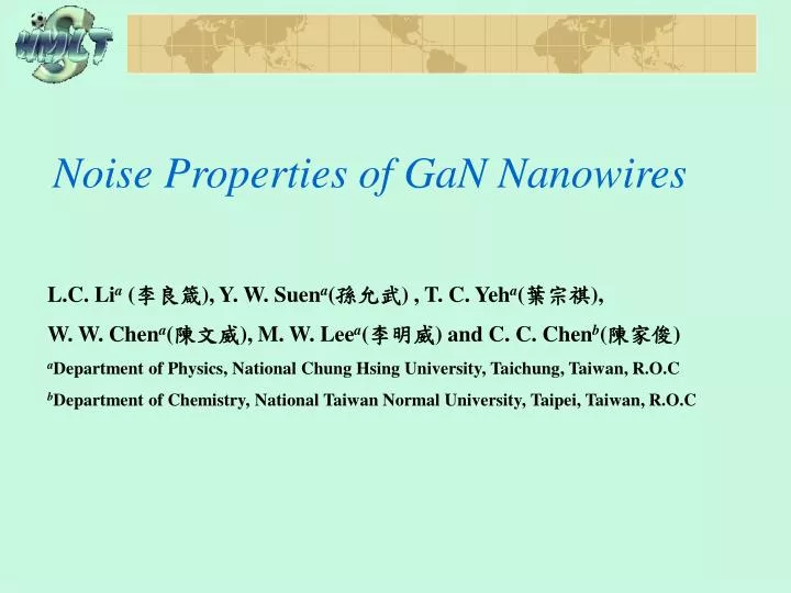
Noise Properties of GaN Nanowires. L.C. Li a ( 李良箴 ), Y. W. Suen a ( 孫允武 ) , T. C. Yeh a ( 葉宗祺 ), W. W. Chen a ( 陳文威 ), M. W. Lee a ( 李明威 ) and C. C. Chen b ( 陳家俊 ) a Department of Physics, National Chung Hsing University, Taichung, Taiwan, R.O.C

E N D
Noise Properties of GaN Nanowires L.C. Lia (李良箴), Y. W. Suena(孫允武) , T. C. Yeha(葉宗祺), W. W. Chena(陳文威), M. W. Leea(李明威) and C. C. Chenb(陳家俊) aDepartment of Physics, National Chung Hsing University, Taichung, Taiwan, R.O.C bDepartment of Chemistry, National Taiwan Normal University, Taipei, Taiwan, R.O.C
Abstract • We will report the noise behavior of GaN nanowires at the room temperature. The typical resistances of the samples are from few kW to hundreds of kW at room temperature. The resistance increases to few MW at 77K. We use cross spectrum and FFT technique to measure the noise properties of these nanowires. The GaN nanowires exhibit the 1/f noise in the current range, 0.1nA ~70nA. The Hooge parameter of the 1/f noise of these wires is around 1.
Introduction • The fluctuation of the condense matter links to the physical phenomena. The 1/f noise arises due to the relaxation of the defects or the dynamics of groups of defects in a finite relaxation time. That means the study of 1/f noise is an issue to understand the physical properties of the condense matter.[1][2] • For the conventional electronic material, the magnitude of the 1/f noise would take into consideration in assessing the potential for electronic and sensor application. • In recent years, the carbon nanotube is a well-studied mesoscopic device. There is the large magnitude of the noise observed.[3][4][5] • It is important to study the 1/f noise of the GaN nanowires. Apart from evaluating the potential of this nanowire as a device, the physical phenomena are worthy to understand.
The 1/f Noise--The Brief Review • It is indicated that the 1/f noise is the noise which is relative to the frequency.[6] only when a=1, b=0, g is dimensionless. where NC is the number of charge carries. g=210-3 in metal and semiconductor.[1] • In the carbon nanotube experiment, the formula is applied: where A is called noise magnitude.[3] A=10-11R b=1~1.1 for Single Wall Nanotube (SWNT) . • For an individual Multiwalled Carbon Nanotube (MWNT), b=1.02. For tow crossing Multiwalled Carbon Nanotube (MWNT), b=1.56 .[5] • In our experiment, we measured the 1/f noise for the frequency below 50Hz. Our results show that the GaN nanowires also exhibit the 1/f-like excess noise. We also note that the 1/f noise of the nanowires exists in a lower frequency range than that of the carbon nanotubes.
Experimental Setup • In this experiment, we use a balanced circuit to measure the noise of an GaN nanowire. There are two methods in our measurement. One is the cross spectrum technique. The other is using the FFT technique directly. We use the SR780 spectrum analyzer. • The specification of our instruments: 1.Homemade JFET-input low-noise voltage preamplifier[7]: Noise: (with very high input impedance) If the cross spectrum technique is used, the noise will be down to 2.SR560 Low-noise preamplifier: Noise 3.SR780 Spectrum Analyzer: Full span: 102.4kHz • The measurable bandwidth is decreased as the resistant of the sample is increased. Even though the 1/f noise we study is below 50Hz, the bandwidth still be carefully checked.
SR780 + - Sample - Fig.1 + Experimental Setup I– Cross Spectrum Measurement • The Fig. 1 is shown the symmetry circuit. The amplifiers are including the homemade JFET preamplifiers and the SR560 low noise preamplifiers. By the use of the two synchronous sampling channels of the SR780 spectrum analyzer, the cross spectrum can be obtained.
+ SR780 Sample - Fig.2 Experimental Setup II– FFT Measurement • In the direct FFT measurement, the amplified signal is directly fed into the SR780. The data can be calculated by the spectrum analyzer in the power spectrum density unit.
Experimental Setup--The Calculation • From the small signal equivalent circuit (Fig.3) of our measurement setup, we can obtain: • Where R=[(R1+R2)//R3//(R4+R5)]+R6+R7 • This illustrates that we should carefully check which one is the dominant noise, when we choose the resistor parallel to the sample. Fig.3
Fig.4 Sample • The nanowire samples are provided by Dr.C. C. Chen of the Department of Chemistry in the National Taiwan Normal University. The nanowires are grown by the Vapor-Liquid-Solid (VLS)method. By applying different metal nanoparticles as the accelerant, the Ga bulk is put into the quartz tube and heated to 910℃ in an increasing rate 50℃ /min. The flow of NH3 is controlled at 18 sccm. The reaction time is 12hours. [8][9] • The electrodes of the nanowires are defined by the e-beam lithography. The Ti/Au is chosen as the ohmic contact for these wires. The device is made by Dr. M.W. Lee’s laboratory. • The fig.4 is the SEM image of the sample 7-1-1.
Sample -- The electric property • Fig.5 is the I-V plots of two samples at the room temperature. The resistant are 34kW and 872.866kW, respectively, by use of the slope from the linear fitting. Fig.5
Fig.6 System Background Noise • It is important to calibrate the system background noise. As the graphs shown, the background noise is smaller than 1× 10-16 V2/Hz. For our samples, the resistant is from 104W to 106W and the typical thermal noise is from 10-16 V2/Hz to 10-14 V2/Hz, respectively. Therefore, this system is good enough to measure the noise.
Fig.7 Results-- The noise of the metal film resistors • The metal film resistors are taken as the standard samples in this experiment. We take these resistors which resistant is about the same as the resistant of the GaN nanowires. The pink line in the plot is the thermal noise of the resistors. From the figure, the data indicates that the metal film resistor has very small 1/f noise when the external current is applied.
Results-- The spectrum of the sample • The nanowire is different from the metal film resistor. There is excess noise raising up when the current through the GaN-nanowire is increased. The orange straight line the plot is the basic thermal noise.
Results-- The Hooge parameter of the Samples • The Hooge parameter is obtained from the data between 0.5Hz and 8Hz.. • For R=34.205kW (sample 7-1-1), the average Hooge parameter is 1.007± 0.045 in I>30nA. For R=872.866kW (sample 7-2-1), the average Hooge parameter of the sample7-2-1 is 1.097± 0.084 in I>0.835nA.
Conclusion • Comparing the noise of the metal film resistor with the noise of the GaN nanowires, the GaN nanowires clearly exhibit the excess 1/f noise. • The smaller resistant of the GaN nanowire is, the lower frequency the 1/f noise is exhibited in. • We measure the 1/f noise of the GaN nanowire in the current range, 0.1nA~100nA. In the bandwidth from 0.5Hz to 8Hz at the room temperature, the Hooge parameter is very close to one.
References • P. Dutta and P. M. Horn, Rev. Mod. Phys. 53, 497 (1981). • A. K. Raychaudhuri, Curr. Opin. Solid State Mater. Sci. 6, 67 (2002). • P. G. Collins, M. S. Fuhrer, and A. Zettl, Appl. Phys. Lett. 76, 894 (2000). • E. S. Snow, J. P. Novak, M. D. Lay, and F. K. Perkins, Appl. Phys. Lett. 85, 4172(2004). F. N. • H. Ouacha, M. Willander, H. Y. Yu, Y. W. Park, M. S. Kabir, S. H. Magnus Persson, L. B. Kish, and A. Ouacha, Appl. Phys. Lett. 80, 1055 (2002). • Hooge, Phys. Lett. A 29, 139 (1969). • 王文凱, 低雜訊前級放大器製作與雜訊之量測, 國立中興大學物理系大學部畢業論文 (2001) • C.C.Chen, C.C.Yeh, C.H.Chen, M.Y.Yu, H.L.Liu, J.J.Wu, K.H.Chen, J.Y.Peng, Y.F.Chen, J. Am. Chem. Soc. 123, 2791. (2001) • S.Dhara, A.Datta, C.T.Wu, Z.H.Chen, Y.L.Wang, L.C.Chen, C.W.Hsu,H.M.Lin, C.C.Chen, Appl. Phys. Lett. 82, 451.