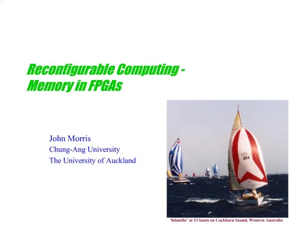
Download
1 / 21
240 likes | 593 Views
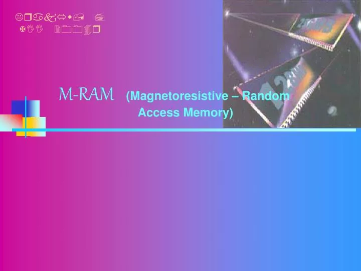
Kraków, 7 XII 2004r. M-RAM (Magnetoresistive – Random Access Memory). Information flux. Information transmission. Information Processing. Information storage. Information. Input. Outside word. Output. Magnetic (HDD) Optical (CD, DVD). DRAM, MRAM.

E N D
Kraków, 7 XII 2004r M-RAM(Magnetoresistive – Random Access Memory)
Information flux. Information transmission Information Processing Information storage Information Input Outside word Output Magnetic (HDD) Optical (CD, DVD) DRAM, MRAM M-RAM M. Bernacki, S. Wąsek
Memory categories. WHY DO WEE NEED M-RAM MEMORY ???? M-RAM M. Bernacki, S. Wąsek
Basic attractions of M-RAM. • Nonvolatility; • Speed; • Low-power consumption; • Scalability. M-RAM M. Bernacki, S. Wąsek
Basic attractions of M-RAM. Transfer data to microprocessor without creating a bottleneck! M-RAM M. Bernacki, S. Wąsek
History and development... • M-RAM – quick view. • Magnetoresistivity. M-RAM based on: • AMR effect - 80-th. • GMR effect - 80-th. • TMR effect – 1995 year. M-RAM M. Bernacki, S. Wąsek
Storage and states of a bit. MRAM: charge and spin. Storage state: • DRAM: charge of capacitor. • Flash, EEPROM: charge on floating gate. • FeRAM: charge of a ferroelectric capacitor. Soft ferromagnet „1” Insulator Hard ferromagnet TMR [%] „0” Field [Oe] M-RAM M. Bernacki, S. Wąsek
Implementationof 1-MTJ / 1-transistor cell. NiFe (free layer) Al2O3 (tunneling barrier) CoFe (fixed layer) SAF Ru CoFe (pinned layer) Word line M-RAM M. Bernacki, S. Wąsek
Write. Word line Without digit line current With digit line current M-RAM M. Bernacki, S. Wąsek
Write. RA [kOhm-um2] Word line Easy axis field [Oe] M-RAM M. Bernacki, S. Wąsek
Read. Word line Word line M-RAM M. Bernacki, S. Wąsek
Sizes of MTJ. Ferromagnet I 4nm NiFe (free layer) 1..2nm Al2O3 (tunneling barrier) Tunnel barrier 3nm CoFe (fixed layer) Ru 3nm CoFe (pinned layer) Ferromagnet II M-RAM M. Bernacki, S. Wąsek
Other MRAM cell architectures. Twin cell arrays: • Circuit is faster than the 1T1TMR implementation. • Less atractive on a cell density and cost basis. Diode cell: • SOI diodes allow the integration of a memory with most circuits without sacrificing silicon wafer surface area. • SOI diodes suitable for this aplication haven’t been developed yet. Transistorless array: • Large reduce in cell area. • Complex circuity required to read bit state, slow read. M-RAM M. Bernacki, S. Wąsek
MRAM 32Kb memory segment. Bit line 0 Bit line 31 Digit line Word line Word line Digit line M-RAM M. Bernacki, S. Wąsek
Reference generator. RMAX RMIN Bit line Digit line Word line Wordline Digit line RMAX RMIN RREF = 1/2(RMAX + RMIN) M-RAM M. Bernacki, S. Wąsek
1Mb MRAM architecture. Available modes: • Active mode • Sleep mode • Standby mode M-RAM M. Bernacki, S. Wąsek
Examples and performance of M-RAM technology. • Motorola semiconductors –2002. • Freescale semiconductors –2003/2004. • Technology: 0.6um, 5-level metal CMOS, copper interconnects; • Capacity: 1MB • Access time: 35ns • Technology: 0.18mikrons, 5-level metal CMOS, copper interconnects; • Capacity: 4MB; • Access time: 15-20ns M-RAM M. Bernacki, S. Wąsek
Roadmap to future storage technologies. RRAM with CMR M-RAM M. Bernacki, S. Wąsek
Bio – MRAM,vision for tomorrow? Biomolecule labeled by magnetic markers MRAM array M-RAM M. Bernacki, S. Wąsek
References. • Wykład z przedmiotu „Magnetyczne nośniki pamięci”, AGH; • Materiały z Uniwersytetu Bielefeld: wykład „Thin films and nanostructures”; • Materiały seminaryjne z „Motorola Labs”; • Materiały z sympozjum „VLSI symposium 2002”; • www.freescale.com • www.motorola.com M-RAM M. Bernacki, S. Wąsek
Dziękujemy za uwagę M-RAM M. Bernacki, S. Wąsek