Download
1 / 23
821 likes | 2.39k Views
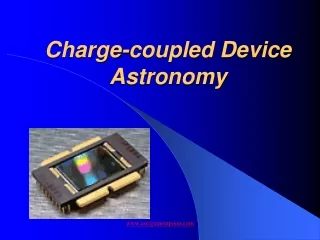
Charge-coupled Devices. (CCDs) Colt Wilkens. History. Invented in 1969 at AT&T Bell Labs First working CCD was an 8-bit shift register By 1964: linear 500-element device, and 2D 100x100 pixel device CCD technology was superior to CMOS. Basic Operation. Uses:

E N D
Charge-coupledDevices (CCDs) Colt Wilkens
History • Invented in 1969 at AT&T Bell Labs • First working CCD was an 8-bit shift register • By 1964: linear 500-element device, and • 2D 100x100 pixel device • CCD technology was superior to CMOS
Basic Operation • Uses: • As a memory (shift register) • A delay line • Imaging devices Source: http://en.wikipedia.org/wiki/File:CCD_charge_transfer_animation.gif
Charge generation • Four causes: • Photo-generation • Generation in the depletion region • Generation at the surface • Generation in the neutral bulk • Photo-generation is the most useful • Quantum efficiency: rate of electrons generated • The other three create “dark-current” (noise)
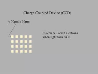
Operating with photons • Channel stop: used to isolate charges into columns • Electrons are captured in the n-well created by the positive gate voltage Source: http://www.microscopyu.com/articles/digitalimaging/ccdintro.html
Illumination Direction Source: http://www.specinst.com/What_Is_A_CCD.html
Quantum Efficiency: Front Source: http://www.specinst.com/What_Is_A_CCD.html
Quantum Efficiency: Back Source: http://www.specinst.com/What_Is_A_CCD.html
Illumination Direction • Backside requires: Thinned Si • Anti-glare coating • Frontside requires: • Basic substrate • Nothing more! Source: http://www.micro.magnet.fsu.edu/primer/digitalimaging/concepts/quantumefficiency.html
Modern Design • Overflow drain: Prevents charge from entering other pixels • Buried channel: accumulated charge is kept from surface; • more transfer efficiency, • lower dark current, • smaller charge cap.
Moving charges in a grid Source: http://www.microscopyu.com/articles/digitalimaging/ccdintro.html
How do they all come together? • First CCD architecture: Full frame • Entire grid read off at once (slow), best with mechanical shutter • Second CCD architecture: Frame transfer • Entire grid shifted to a storage array (quick),then read off from storage array • Required twice the space for same image
The compromise • Third CCD architecture: inter-line • Every other line is storage, only one pixel shift • Half of the light is blocked, fill factor down 50% • (same with quantum efficiency) • Modern microlenses solve the fill factor issue
Comparison between architectures Source: http://www.microscopyu.com/articles/digitalimaging/ccdintro.html
Solving the flaw of interline Microlenses help capture light near storage cells and focus it on the right location Source: http://www.microscopyu.com/articles/digitalimaging/ccdintro.html
Architectures today • Frame-transfer was a common choice before interline was viable, still useful where interline can’t be used (back illumination) • Full-frame is best at light collection: primarily used in astronomy • Interline is quick and cheap: primarily used in consumer products
Sidenote: Astronomy Use • Multiple exposures: images with shutter closed subtracted from open shutter images, to remove dark current, thermal noise and cosmic rays • Drift-scanning: reading charges in parallel with the sky movement, at the same speed, to make a fixed telescope behave like a tracking telescope • Right: 30 CCDs on the Sloan Digital Sky Survey telescope Source: http://www.sdss.org/dr6/instruments/imager/index.html
Moving charges in a CCD Source: http://www.micro.magnet.fsu.edu/primer/digitalimaging/
How do we get color? • Bayer mask: twice as many green to mimic human sensitivity • Trichroic beam splitter prism, and 3 CCDs Source: http://en.wikipedia.org/wiki/Charge-coupled_device
Other imaging tech: CMOS • CMOS: array of photodetectors and active amplifiers • Less expensive • Need less power • “rolling shutter” effect is unwanted • CCD: photons to electrons guided by potential wells • More accurate light detection • unwanted “blooming” effect is worse
Intensified CCD • Image intensifier mounted in front of the CCD • Photocathode: photons → electrons • Micro-channel plate: multiplies electrons • Phosphor screen: electrons → photons • Reversing voltage on MCP: reverses electrons, “gating” the CCD • Advantages • High light sensitivity • Single photon detection • Shutter times of ~200 picoseconds
Electron-multiplying CCD • Gain register is added before output amplifier • High gain causes noise, so more suitable for low light conditions • Requires a cooling system: -65°C to -95°C • EMCCDs are better for low light • ICCDs are better for high speed