Download
1 / 66
710 likes | 915 Views
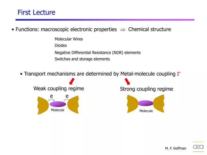
e. Strong coupling regime. e. Molecule. First Lecture. Chemical structure. Functions: macroscopic electronic properties . Molecular Wires. Diodes. Negative Differential Resistance (NDR) elements. Switches and storage elements.

E N D
e Strong coupling regime e Molecule First Lecture Chemical structure • Functions: macroscopic electronic properties Molecular Wires Diodes Negative Differential Resistance (NDR) elements Switches and storage elements • Transport mechanisms are determined by Metal-molecule coupling G Weak coupling regime Molecule
e Strong coupling regime e Molecule 2 1 3 Second Lecture Chemical structure • Functions: macroscopic electronic properties Molecular Wires Diodes Negative Differential Resistance (NDR) elements Switches and storage elements • Transport mechanisms are determined by Metal-molecule coupling G Weak coupling regime Molecule Qualitative Picture Final Remarks
Molecular Conduction: Qualitative Picture Two Basic Ingredients: Energy Diagram showing the molecular levels relative to the electrochemical potential of electrodes Potential Profile across the molecule due to the applied bias.
Chemically bonded G Mdn E G Fermi level µF Local Density of States Broadening of the energy levels (G) Discrete Energy Levels M0Mdn Fractional charge transfer Strong Coupling to Metallic Electrodes (G) Isolated Molecule M0 E LUMO HOMO Which is the location µF with respect to HOMO-LUMO levels?
E Local Density of States Location of the Fermi Energy UPS Experiments (UV Photo Electron Spectroscopy ) Vacuum Level UPS spectrum e- µF # e per second e- µF E Vacuum Level e- G HOMO # e per second Mdn µF E EHOMO e-
e- S S CH3COSe SeCOCH3 S e- UPS Experiment on Self-assembled Monolayer on Au Se3
Energy Diagram At equilibrium (V=0) -V/2 R V/2 L R L µ L µ L=µR eV µR But how are µL and µR disposed with respect to the molecular levels? Potential profile inside the molecule
-V/2 R V/2 L Potential Profile V/2 Potential Profile -V/2 r To the lowest approximation Molecular Levels shift "rigidly" by Let us denote this average potential as: Taking the molecular levels as our reference, the electrochemical potential of electrodes are shifted by This voltage division factor has a profound effect on Current-Voltage Characteristics
Energy Level Diagram (=0) =0 Molecular levels remain fixed to µ L µR LUMO LUMO µ L µ L eV eV µR HOMO HOMO V<0 LUMO Conduction V>0 HOMO Conduction I-V Characteristics can look asymetric Positive branch (V>0) and Negative branch (V<0) involve different Molecular levels
LUMO LUMO µ L µR µ L eV/2 eV/2 µR HOMO HOMO Energy Level Diagram (=1/2) =1/2 Molecular levels shift with respect to µ L by half the applied bias Conductiontakesplacethroughthenearestmolecular level (HOMO in this case) for either bias polarity.
R L G e Toy Model Toy Moldel: single level e (HOMO or LUMO) that incorporates relevant ingredients: (1) Location of e with respect to µF (2) Broadening GL,GR due to contacts (G=GL+GR) (3) Potential Profile µ L µR
-V/2 R V/2 L µR Current as a "balancing act" Discrete One-Level Model GR GL µ L e
-V/2 R V/2 L Discrete One-Level Model GR GL µ L e The net flux across left junction will be
-V/2 R V/2 L µR Discrete One-Level Model GR GL The net flux across right junction will be e
Discrete One-Level Model At the steady state IL+IR=0 (no charge accumulation in the molecule) The current through the metal-molecule-metal structure will be
µ L µ L µ L µR µR µR One-level Model: Current (I) vs. Voltage (V) e Let us take into account Broadening G of the level
Broadening G We replace the discrete level by a Lorentzian density of states: µ L µR G e Expression of the current will be modified We could write in the Landauer-Büttiker form I let for you the demostration that the maximum value of
G One-level Model: Current (I) vs. Voltage (V) Conductance Quantum Next: Potential Profile
-V/2 R V/2 L CL CR -V/2 V/2 Potential Profile The potential profile VMOL(r) will be obtained by solving A solution can be visualized in terms of a capacitance circuit model: The potential U that raises the position of the level is Charging Energy Eadd
Self Consistent Solution Iterative Procedure for calculating N and U self-consistently
µ L µ L µR µR V<0 V>0 Positively charges the molecule shift e down One-level Model: Current (I) vs. Voltage (V) IV asymetric Coupling asymetry + charging e
G Summary Asymetric IVs asymetric coupling + charging effect (Eadd) even if transport is associated with a single level (symetric molecule) HOMO conduction I is lower for positive bias on the stronger contact LUMO conduction I is higher for positive bias on the stronger contact • I increases when e is crossed at V~2(µF-e) • I increases over a voltage width G+kBT • I dragged out by charging Eadd
Realistic Models Non-Equilibrium Green's Function (NEGF) Formalism Let us rewritte the previous eq. in terms of a Green Function G(E) Then the density of states will be proportional to the so called Spectral function defined as The mean number of excess electrons N and the current can be written as
NEGF Formalism For a multilevel Molecule (n levels) all quantities are replaced by a corresponding matrix (n x n ) H : Molecule + surface atoms S : Coupling to bulk contacts U : appropriate functional A pedagogical tutorial: S. Datta, Nanotechnology 15, S433 (2004).
Experiments on Molecular Wires Well coupled to electrodes (at least one of them)
L~nm A) How conductance depends on the length L of the wire? B) How conductance depends on the binding group of the wire? C) How conductance depends on the structure of the wire? Molecular Wires Large delocalized p systems Conductance is a property of the Metal-Molecule-Metal structure
How one can measure transport properties of molecular wires? 1) STM: Scanning Tunneling Microscope 2) Break-junctions Mechanically controlled Electronmigration-induced 3) Shadow evaporation on Self-assembled Monolayers (SAMs)
Tip s s s s s s s s s Adsorption MBE: Molecular "Beaker" Epitaxy Au (111) Solution Thiol-ended Molecules Au (111) STM Image Organization
Conductive AFM on Self-Assembled Monolayers Sakaguchi et al., APL 2001 Measured g=0.41Å-1 for oligothiophene g=1.08 Å-1 for alkanethiol Theory g=0.33Å-1 for oligothiophene g=1.0 Å-1 for alkanethiol
STM on specially designed molecular wire Langlais et al., PRL 1999 Conductance depends exponentially onL
M. P. Samanta et al., PRB 53, R7626 (1996). µ L eV µR Explanation V/2 -V/2 L R At low voltages µF is far from HOMO and/or LUMO Tunneling Transmission
B) How conductance depends on the bindinggroup of the molecular wire?
S S CH3COX X S Influence of thebindinggroupof electroactive molecules X = S or Se Theoretical studies Conductance of molecular wires: Influence of molecule-electrode binding. S.N. Yaliraki, M. Kemp, and M.A. Ratner, J. Am. Chem. Soc. 121(14), 3428 (1999) Se > S Molecular alligator clips for single molecule electronics. Studies of group 16 and isonitriles interfaced with Au contacts. J.M. Seminario, A.G. Zacarias, and J.M. Tour J. Am. Chem. Soc. 121(2), 411 (1999) S > Se Experiments are needed X=S T3 X=Se Se3
Investigation of T3 and Se3 S S T3 CH3COS SCOCH3 S Se3 quite similar IPs “Identical” HOMOs S S CH3COSe SeCOCH3 S 6.50 eV 6.52 eV Se3 T3 Influence of the binding group: Se vs S
Adsorption Sample Preparation Au (111) Insertion Solution Thiol-ended Insulating Molecules Solution Conducting Molecules Organization
T3 S S CH3COS SCOCH3 S Se3 S S CH3COSe SeCOCH3 S h x Molecular structure - transport properties relationship STM tip L. Patrone et al, Chem. Phys.281(2002)325 PRL 91(03) 096802 28 nm T3,Vt = +0.78V, It = 10.7pA
T3 S S CH3COS SCOCH3 S Se3 S S CH3COSe SeCOCH3 S h x Molecular structure - transport properties relationship STM tip L. Patrone et al, Chem. Phys.281(2002)325 PRL 91(03) 096802 28 nm T3,Vt = +0.78V, It = 10.7pA
T3 S S CH3COS SCOCH3 S Se3 S S CH3COSe SeCOCH3 S h x Molecular structure - transport properties relationship STM tip L. Patrone et al, Chem. Phys.281(2002)325 PRL 91(03) 096802 The apparent height is a (relative) measure of the conductance of the molecular junction 28 nm T3,Vt = +0.78V, It = 10.7pA
Topography: 1.0 nm T3 Topography: 1.0 nm Se3 S vs Se: Experimental comparison STM on T3 and Se3 Molecules inserted in a dodecanethiol Matrix L. Patrone et al, Chem. Phys. 281(2002)325 STM tip It It 28 nm T3,Vt = +0.78V, It = 10.7pA
Se3 (Se) T3 (S) Se3 > T3 S vs Se: Experimental comparison Se give rise to a more efficient transport than S
T3 V eV 2(EF-EHOMO) Position of the HOMO level/ Fermi level (EF-EHOMO) : T3 > (EF-EHOMO) : Se3 Current-Voltage characteristic I I Se3 LUMO HOMO EF EF-EHOMO eV
Position of the HOMO / Fermi level UPS (UV Photoelectron Spectroscopy) 1 monolayer adsorbed onto gold T3 :EF-EHOMO> Se3:EF-EHOMO
C) How conductance depends on the structure of the wire?
C) Comparaison of backbone conductance Kushmeric, Ratner et al JACS 2003 OPV > OPE OPV vs Othiophene?
(15.6 Å) S S T3 CH3COS SCOCH3 S CH3COS OPV2 (12.67 Å) SCOCH3 CH3COS OPV2 :HOMO - EF 0.7 eV OPV3:HOMO - EF 0.35-0.7 eV SCOCH3 C) Influence of the conjugated body: T3 vs OPVn 2.0 Å 4.2 Å OPV3 (19.04 Å) 7.3 Å OPVs are more conducting than Othiophene
Which is the IV characteristic of a Metal-single molecule-Metal device?
Tip Metallic substrate Single Molecule Measurement Conducting AFM on Alkanedithiol on a alkanethiol matrix X.D. Cui et al., Science 2001.
Single Molecule Measurement Conductance histograms with STM N. J. Tao, Science 2003.
Contacting Single Molecules Mechanically Controlled break-junctions J. M. van Ruitenbeek et al Rev. Sci. Instrum. 67 (1995) 108 Advantages High stability accuracy dl/Dz~10-5 Freshly exposed metal surfaces dl Drawbacks No image of contacted molecules No gating Dz