Download
1 / 23
230 likes | 236 Views
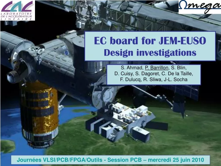
EC board for JEM-EUSO Design investigations. S. Ahmad, P. Barrillon , S. Blin, D. Cuisy, S. Dagoret, C. De la Taille, F. Dulucq, R. Sliwa, J-L. Socha. Journées VLSI/PCB/FPGA/Outils - Session PCB – mercredi 25 juin 2010. JEM – EUSO. Charged Particles. EECR s. Dust and Meteors.

E N D
EC board for JEM-EUSODesign investigations S. Ahmad, P. Barrillon, S. Blin, D. Cuisy, S. Dagoret, C. De la Taille, F. Dulucq, R. Sliwa, J-L. Socha Journées VLSI/PCB/FPGA/Outils - Session PCB – mercredi 25 juin 2010
JEM – EUSO Charged Particles EECRs Dust and Meteors Ultraviolet photons UV, X, γ,ν p, n, e X, γ,ν,p, e Atmosphere Solar wind Air shower Air shower The Earth Night glow Plasma Discharge • Satellite project (not yet approved) that should be installed on International Spatial Station (~ 2015) • International collaboration (East Asia, EU, US) supported by 3 spatial agencies (JAXA, NASA, ESA) • Multi-purpose experiment • Study of cosmic rays and their sources • Study of atmospheric physic • Study of meteors • Lightning study… Journees VLSI/PCB/FPGA/Outils - Session PCB - Pierre Barrillon - LAL
JEM – EUSO detector Focal Surface SPACIROC (See S. Amhad talk) Readout chip PDM 5000 MAPMTs (8x8 pixels) Journees VLSI/PCB/FPGA/Outils - Session PCB - Pierre Barrillon - LAL
EC board – next generation PMF PMF exploded view active board lumi pmf2 alpha passive board lumi pmf passive Big insulating Small insulating lumi pmf HV 0715 Small insulating Big insulating hv board PMT MAPMT H7546 from Hamamatsu See talk given 2 years ago • Study of EC board has been asked to LAL • Power MAPMTs • SPACIROC location • Data transfer to the rest of electronic line • Starting point: PMF (PhotoMultiplier Front end) - Front end electronic for ATLAS luminometer (ALFA) used to readout 64 channels MAPMTs from Hamamatsu • 3 PCB boards (3 x 3 cm) are used: • HV board: allows bringing high voltage to the MAPMT (64ch) • Passive board: roots signals to connectors on the edges of the board • Active board: readout and treatment of the PM output signals successively by the MAROC2 ASIC on one side and a Lattice FPGA on the other side. FPGA side kapton cable ASIC side 3.5 cm PMT Journees VLSI/PCB/FPGA/Outils - Session PCB - Pierre Barrillon - LAL
Mechanical constraints (1) Electronics + Supports + Volume for Electronics (167 x 128 x 130) Frame + MAPMT+ Electronics PDM Frame EC Base MAPMT PDM frame: 167mm x 167mm x 28.7mm Journees VLSI/PCB/FPGA/Outils - Session PCB - Pierre Barrillon - LAL
Mechanical constraints (2) 28.7 192.4 130 167 128 Considering all dimensions we have a really limited space available (in thickness) for the EC board (4-5 mm) + frame: ~ 12 mm Can not have 3 PCBs (like PMF) MAPMT Journees VLSI/PCB/FPGA/Outils - Session PCB - Pierre Barrillon - LAL
Starting point: EC board dimensions • 52.5 mmx 52.5 mm (frame: 55 x 55) Hole dedicated to the rod used for fixing Frame (drawings from INFN Frascati) LAL drawing for EC board Journees VLSI/PCB/FPGA/Outils - Session PCB - Pierre Barrillon - LAL
64 channels MAPMT dimensions Vacuum pipe present for the prototype removed for production 14 pins needed: dynodes 1 to 12 + GR + K Journees VLSI/PCB/FPGA/Outils - Session PCB - Pierre Barrillon - LAL
EC board design considered • Single thick PCB since 3 PCB-like is not possible because of space constraint • Readout ASIC in a BGA package mounted on the other side of the PCB • BGA looks like a good solution considering the tight space constraints • BGA should be chosen considering the foreseen (higher estimation) number of I/O and the space available • MAPMT pins inserted in the PCB into non-crossing holtites • 1 connector would bring all signals (14) needed by the MAPMT • 2 connectors (60 pins foreseen) would bring power to the ASIC and collect output signals • Easier to drive the signals to/from the 4 ASICs • Good connection reliability Journees VLSI/PCB/FPGA/Outils - Session PCB - Pierre Barrillon - LAL
BGA 144 pins BGA (13 x 13 mm) 1 mm step 2 ways to connect the chip inside BGA • Number of pins should be enough considering similar ASICs • Dimensions are reasonable and give more space to locate the connectors R. Sliwa Journees VLSI/PCB/FPGA/Outils - Session PCB - Pierre Barrillon - LAL
Overall view J-L Socha CMS connector 22 signals + power CMS connector 22 signals + power Estimated from frame drawing HV connector (14 lines) Journees VLSI/PCB/FPGA/Outils - Session PCB - Pierre Barrillon - LAL
PCB structure Length needed for MAPMT pins: 7 mm (5.6 mm on proto) Example of PCB structure (mm) Type of vias considered Journees VLSI/PCB/FPGA/Outils - Session PCB - Pierre Barrillon - LAL
MAPMT print + bottom view Some of the pins (HV) are really close to the edges, we would need more space rotated x 4 and located in the considered design of the EC board 0.5 mm is the minimum distance between hole and edge of PCB HV instability with PDM frame ? 8 pins would be on the edges… but only 2 could be used little modification of the frame design Journees VLSI/PCB/FPGA/Outils - Session PCB - Pierre Barrillon - LAL
Top view Connector print BGA print Journees VLSI/PCB/FPGA/Outils - Session PCB - Pierre Barrillon - LAL
Conclusion • First steps of EC board design: • Feasibility • non crossing holtites only one company (pretend to) do it in France • chip in BGA • Dimensions taking into account: • MAPMT dimensions • BGA size • location for connectors • Some needs (length of PMT pins and size of the PCB) • Many other steps to come • single thick PCB (can mean large vias), ok for space ? … • This is a very innovative concept and challenging project. We don't have the experience return with this technology (thick PCB and non-crossing holtites) • We will need to try several options starting with a mockup version that would be useful to check feasibility mechanically and electronically (money expected to develop these various prototypes) • It looks like the only option that fits the JEM-EUSO space and spatial constraints and probably reliability • First adaptations of the EC frame have been applied following our comments Journees VLSI/PCB/FPGA/Outils - Session PCB - Pierre Barrillon - LAL
Changes on the frame Journees VLSI/PCB/FPGA/Outils - Session PCB - Pierre Barrillon - LAL
BACK-UP SLIDES Journees VLSI/PCB/FPGA/Outils - Session PCB - Pierre Barrillon - LAL
From where the 4mm come MAPMT location EC board location Total thickness of the frame 6.5 – 2 – 0.5 = 4 mm Journees VLSI/PCB/FPGA/Outils - Session PCB - Pierre Barrillon - LAL
HOLTITE Journees VLSI/PCB/FPGA/Outils - Session PCB - Pierre Barrillon - LAL
PMF structure MAROC side Lattice side HV board Passive board Active board • The PCB part of the PMF is made of 3 boards (3 × 3 cm2) : • HV board: allows bringing high voltage to the MAPMT (64ch) • Passive board: roots signals to connectors on the edges of the board • Active board: readout and treatment of the PM output signals successively by the MAROC2 ASIC on one side and a Lattice FPGA on the other side. • A 60 points connector allows connection of the PMF with the mother board or the test board thanks to a kapton cable. • The 3 PCBs, the cable and the test board were developed at LAL, the mother board and the Lattice firmware at CERN. Journees VLSI/PCB/FPGA/Outils - Session PCB - Pierre Barrillon - LAL
The HV board • 2 layers (c1 and c2) PCB • Brings high voltage to the PMT Vacuum Large insulating element C2 C1 HV cable 64 channels MAPMT H7546 from Hamamatsu Journees VLSI/PCB/FPGA/Outils - Session PCB - Pierre Barrillon - LAL
The passive board • 4 layers (c1, c2, c3 and c4) PCB • Routes signals from PMT to the connectors on the edge • Routing optimized to reduce cross-talk C1 C2 C3 C4 Holetites inserted and bonded on C1 side Black connectors bonded on C4 side Journees VLSI/PCB/FPGA/Outils - Session PCB - Pierre Barrillon - LAL
The active board C2 Top • Challenging part of the project ! • Design of a 10 layers printed circuit board with MAROC chip bonded (at CERN) directly on the PCB on one side and a FPGA/BGA on the other side. • Different types of crossing, blind and laser vias • Limited space available for the other components (connectors, capacitors, resistors) and the test points • MAROC located on 6th layer • Bonding wires connected to pads located on c1 (top) and c2 layers. Journees VLSI/PCB/FPGA/Outils - Session PCB - Pierre Barrillon - LAL