Download
1 / 1
10 likes | 201 Views
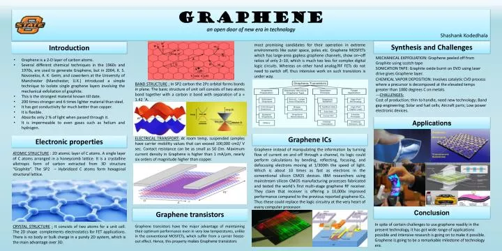
GRAPHENE an open door of new era in technology Shashank Kodedhala. BAND STRUCTURE : In SP2 carbon the 2Pz orbital forms bonds in plane. The basic structure of unit cell consists of two atoms bond together with a carbon

E N D
GRAPHENE an open door of new era in technology Shashank Kodedhala • BAND STRUCTURE: In SP2 carbon the 2Pz orbital forms bonds in plane. The basic structure of unit cell consists of two atoms bond together with a carbon 𝜋 bond with separation of a ≈ 1.42 ˚A. • ELECTRICAL TRANSPORT: At room temp, suspended samples have carrier mobility values that can exceed 100,000 cm2/ V sec. Contact resistance can be as small as 50 Ωm. Maximum current density in Graphene is higher than 1 mA/𝜇m, nearly six orders of magnitude higher than copper. • Graphene transistors have the major advantage of maintaining their optimum performance even in very low temperatures, unlike in the conventional MOSFETs, which suffer from a carrier freeze-out effect. Hence, this propertymakes Graphene transistors most promising candidates for their operation in extreme environments like outer space, poles etc. Graphene MOSFETs which has large-area gapless graphene channels, show on–off ratios of only 2–10, which is much too less for complex digital logic circuits. Whereas on other hand analog/RF FETs do not need to switch off, thus intensive work on such transistors is under way. Graphene instead of manipulating the information by turning flow of current on and off through a channel, its logic could perform calculations by bending, reflecting, focusing, and defocusing electrons moving at 1/300th the speed of light. Which is about 10 times as fast as electrons in the conventional silicon CMOS devices. IBM researchers using mainstream silicon CMOS manufacturing processes fabricated and tested the world's first multi-stage graphene RF receiver.They claim that receiver is offering a 10,000x improved performance compared to the previous reported graphene ICs.Thus these could replace the logic circuitry at the very heart of every computer processor. Synthesis and Challenges Introduction MECHANICAL EXPFOLIATION: Graphene peeled off from Graphite using scotch tape SONICATION TAPE: Graphite oxide burnt on DVD using laser drive gives Graphene layer. CHEMICAL VAPOR DEPOSITION: Involves catalytic CVD processwhere a precursor is decomposed at the elevated temps greater than 1000 degrees C on metals. ---CHALLENGES: Cost of production; thin to handle, need new technology;Band gap engineering;Solar and fuel cells;Aircraft parts; Low power electronic devices. • Graphene is a 2-D layer of carbon atoms. • Several different chemical techniques in the 1960s and 1970s, are used to generate Graphene, but in 2004, K. S. Novoselov, A. K. Geim, and coworkers at the University of Manchester (Manchester, U.K.) introduced a simple technique to isolate single graphene layers involving the mechanical exfoliation of graphite. • This is the strongest material known till date. • 200 times stronger and 6 times lighter material than steel. • It has got conductivity far much better than copper. • It is flexible. • Absorbs only 2 % of light when passed through it. • It is impermeable to even gases such as helium and hydrogen. Applications Graphene ICs Electronic properties • ATOMIC STRUCTURE : 2D atomic layer of C atoms. A single layer of C atoms arranged in a honeycomb lattice. It is a crystalline allotropic form of carbon extracted from 3D structure “Graphite”. The SP2 – Hybridized C atoms form hexagonal structural lattice. • CRYSTAL STRUCTURE: It consists of two atoms for a unit cell. The 2D shape complements electrostatics for FET applications. There is no body or bulk charge in a purely 2D system, which is the main advantage over 3D. Conclusion Graphene transistors In spite of certain challenges to use graphene readily in the present technology, it has got wide range of applications possible and intensive research is going on to make it possible. Graphene is going to be a remarkable milestone of technology era.