Download
1 / 1
10 likes | 138 Views
BEST Back End. Stelio Montebugnoli, Marco Bartolini, Germano Bianchi 1 , Giovanni Naldi 2 , Jason Manley 3 , Aaron Parsons 4. 1 INAF-IRA (I), 2 University of Bologna (I), 3 University of Cape Town (SA), 4 University of California, Berkeley (CA) .

E N D
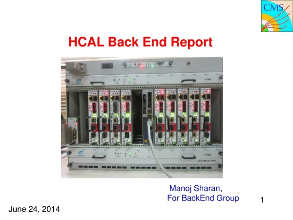
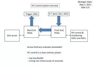
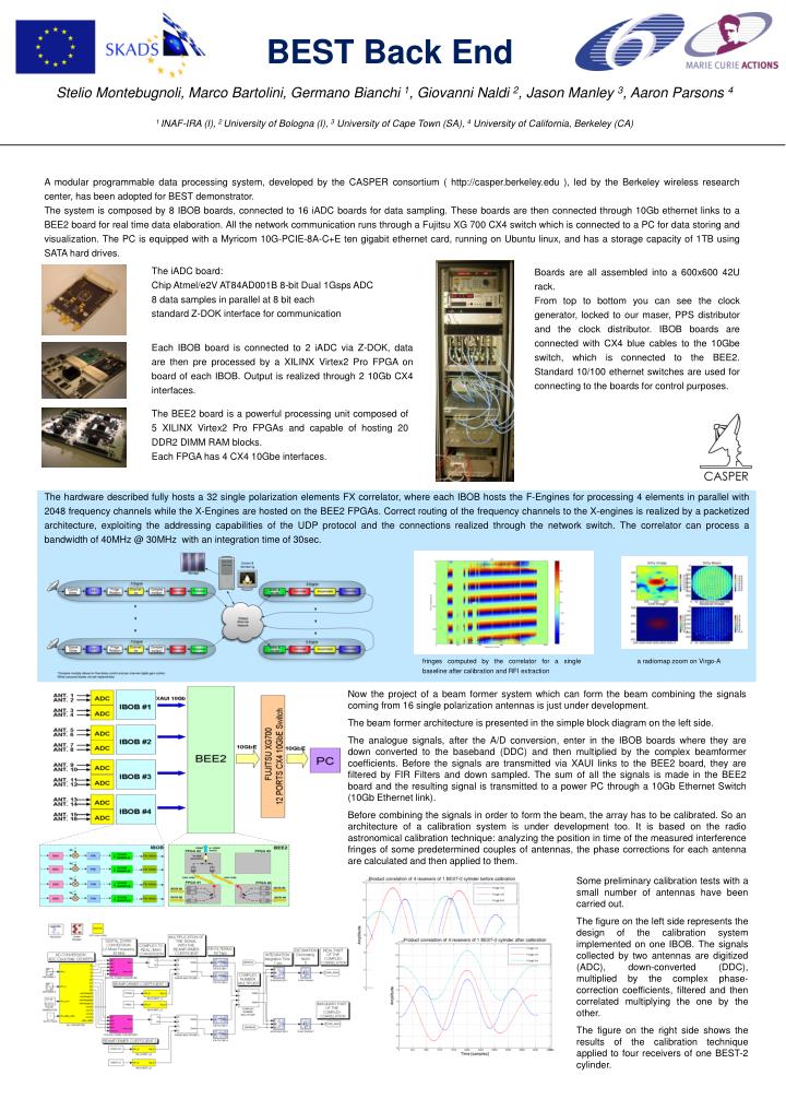
BEST Back End Stelio Montebugnoli, Marco Bartolini, Germano Bianchi 1, Giovanni Naldi 2, Jason Manley 3, Aaron Parsons 4 1 INAF-IRA (I), 2 University of Bologna (I), 3 University of Cape Town (SA), 4 University of California, Berkeley (CA) A modular programmable data processing system, developed by the CASPER consortium ( http://casper.berkeley.edu ), led by the Berkeley wireless research center, has been adopted for BEST demonstrator. The system is composed by 8 IBOB boards, connected to 16 iADC boards for data sampling. These boards are then connected through 10Gb ethernet links to a BEE2 board for real time data elaboration. All the network communication runs through a Fujitsu XG 700 CX4 switch which is connected to a PC for data storing and visualization. The PC is equipped with a Myricom 10G-PCIE-8A-C+E ten gigabit ethernet card, running on Ubuntu linux, and has a storage capacity of 1TB using SATA hard drives. The iADC board: Chip Atmel/e2V AT84AD001B 8-bit Dual 1Gsps ADC 8 data samples in parallel at 8 bit each standard Z-DOK interface for communication Boards are all assembled into a 600x600 42U rack. From top to bottom you can see the clock generator, locked to our maser, PPS distributor and the clock distributor. IBOB boards are connected with CX4 blue cables to the 10Gbe switch, which is connected to the BEE2. Standard 10/100 ethernet switches are used for connecting to the boards for control purposes. Each IBOB board is connected to 2 iADC via Z-DOK, data are then pre processed by a XILINX Virtex2 Pro FPGA on board of each IBOB. Output is realized through 2 10Gb CX4 interfaces. The BEE2 board is a powerful processing unit composed of 5 XILINX Virtex2 Pro FPGAs and capable of hosting 20 DDR2 DIMM RAM blocks. Each FPGA has 4 CX4 10Gbe interfaces. The hardware described fully hosts a 32 single polarization elements FX correlator, where each IBOB hosts the F-Engines for processing 4 elements in parallel with 2048 frequency channels while the X-Engines are hosted on the BEE2 FPGAs. Correct routing of the frequency channels to the X-engines is realized by a packetized architecture, exploiting the addressing capabilities of the UDP protocol and the connections realized through the network switch. The correlator can process a bandwidth of 40MHz @ 30MHz with an integration time of 30sec. fringes computed by the correlator for a single baseline after calibration and RFI extraction a radiomap zoom on Virgo-A Now the project of a beam former system which can form the beam combining the signals coming from 16 single polarization antennas is just under development. The beam former architecture is presented in the simple block diagram on the left side. The analogue signals, after the A/D conversion, enter in the IBOB boards where they are down converted to the baseband (DDC) and then multiplied by the complex beamformer coefficients. Before the signals are transmitted via XAUI links to the BEE2 board, they are filtered by FIR Filters and down sampled. The sum of all the signals is made in the BEE2 board and the resulting signal is transmitted to a power PC through a 10Gb Ethernet Switch (10Gb Ethernet link). Before combining the signals in order to form the beam, the array has to be calibrated. So an architecture of a calibration system is under development too. It is based on the radio astronomical calibration technique: analyzing the position in time of the measured interference fringes of some predetermined couples of antennas, the phase corrections for each antenna are calculated and then applied to them. Some preliminary calibration tests with a small number of antennas have been carried out. The figure on the left side represents the design of the calibration system implemented on one IBOB. The signals collected by two antennas are digitized (ADC), down-converted (DDC), multiplied by the complex phase-correction coefficients, filtered and then correlated multiplying the one by the other. The figure on the right side shows the results of the calibration technique applied to four receivers of one BEST-2 cylinder.