Download
1 / 32
440 likes | 1.04k Views
AFM. Atomic Force Microscopy. Outline. Motivation History How the AFM works Two modes Contact Mode Non-Contact Mode Force Measurements Raster the Tip: Generating an Image Scanning Sample OUr AFM Pictures Examples The Good The Bad And the Ugly Uses Topographical Analysis

E N D
AFM Atomic Force Microscopy
Outline • Motivation • History • How the AFM works • Two modes • Contact Mode • Non-Contact Mode • Force Measurements • Raster the Tip: Generating an Image • Scanning Sample • OUr AFM • Pictures • Examples • The Good • The Bad • And the Ugly • Uses • Topographical Analysis • Thin Layer Depth • RMS Roughness Calculations • Other types of Microscopy
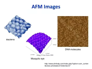
Motivation • Digitally image a topographical surface • Determine the roughness of a surface sample or to measure the thickness of a crystal growth layer • Image non-conducting surfaces such as proteins and DNA • Study the dynamic behavior of living and fixed cells
History • The Scanning Tunneling Microscope (STM) was invented by G. Binnig and H. Rohrer, for which they were awarded the Nobel Prize in 1984 • A few years later, the first Atomic Force Microscope (AFM) was developed by G. Binnig, Ch. Gerber, and C. Quate at Stanford University by gluing a tiny shard of diamond onto one end of a tiny strip of gold foil • Currently AFM is the most common form of scanning probe microscopy
van der Waals force curve How the AFM Works • The AFM brings a probe in close proximity to the surface • The force is detected by the deflection of a spring, usually a cantilever (diving board) • Forces between the probe tip and the sample are sensed to control the distance between the the tip and the sample.
Two Modes Repulsive (contact) • At short probe-sample distances, the forces are repulsive Attractive Force (non-contact) • At large probe-sample distances, the forces are attractive The AFM cantelever can be used to measure both attractive force mode and repulsive forces.
Non-Contact Mode • Uses attractive forces to interact surface with tip • Operates within the van der Waal radii of the atoms • Oscillates cantilever near its resonant frequency (~ 200 kHz) to improve sensitivity • Advantages over contact: no lateral forces, non-destructive/no contamination to sample, etc. van der Waals force curve
Contact Mode • Contact mode operates in the repulsive regime of the van der Waals curve • Tip attached to cantilever with low spring constant (lower than effective spring constant binding the atoms of the sample together). • In ambient conditions there is also a capillary force exerted by the thin water layer present (2-50 nm thick). van der Waals force curve
Force Measurement • The cantilever is designed with a very low spring constant (easy to bend) so it is very sensitive to force. • The laser is focused to reflect off the cantilever and onto the sensor • The position of the beam in the sensor measures the deflection of the cantilever and in turn the force between the tip and the sample.
Raster the Tip: Generating an Image • The tip passes back and forth in a straight line across the sample (think old typewriter or CRT) • In the typical imaging mode, the tip-sample force is held constant by adjusting the vertical position of the tip (feedback). • A topographic image is built up by the computer by recording the vertical position as the tip is rastered across the sample. Scanning Tip Raster Motion Top Image Courtesy of Nanodevices, Inc. (www.nanodevices.com) Bottom Image Courtesy of Stefanie Roes (www.fz-borstel.de/biophysik/ de/methods/afm.html)
Scanning the Sample • Tip brought within nanometers of the sample (van der Waals) • Radius of tip limits the accuracy of analysis/ resolution • Stiffer cantilevers protect against sample damage because they deflect less in response to a small force • This means a more sensitive detection scheme is needed • measure change in resonance frequency and amplitude of oscillation Image courtesy of (www.pacificnanotech.com)
OUr AFM We have a commercial Topometrix Explorer AFM.
Some of Our Pictures 2D topographical image of Atomic Step 3D Image Screw dislocations on InSb grown by MBE
The Good Examples Carbon Nanotube Used as a Conducting AFM Tip for Local Oxidation of Si. View of Silicon Surface Reconstruction Right Image Courtesy of Dai, et al. from Stanford
The Bad Examples Histogram shows level surface, but scan is very streaky Typically the sample will have a slight tilt with respect to the AFM. The AFM can compensate for this tilt. The horizontal lines are due to tip hops – where the tip picks up or loses a small “nanodust” In this image the tilt have not yet been removed.
And the Ugly! Teeny little dust mites, ultra tiny dust mites about 2,000 in the average bed Image courtesy of http://www.micropix.demon.co.uk/sem/dustmite/article/page_2.htm
Topography Scanning Example of generated image upon scanning Pd thermally evaporated on Si
Elimination of Extreme Points This targets the highest points of the sample and eliminates them It then manipulates the image to create a smaller dynamic depth Centering on pt. extreme (Height)
A Better View • Now: • Removed extreme points • Digitally decreased the height of analysis • Less than 1/3 as high as initial scan • Lose resolution and data by clipping off extreme points
Thickness of a Thin Layerof Pd on Si Wafer Si/Pd step Step (where Pd coating ends) Systematic error
Surface Roughness Roughness typically measured as root mean squared (RMS)
Other Types of SPM Techniques • Lateral Force Microscopy (LFM) • Frictional forces measured by twisting or “sideways” forces on cantilever. • Magnetic Force Microscopy (MFM) • Magnetic tip detects magnetic fields/measures magnetic properties of the sample. • Electrostatic Force Microscopy (EFM) • Electrically charged Pt tip detects electric fields/measures dielectric and electrostatic properties of the sample • Chemical Force Microscopy (CFM) • Chemically functionalized tip can interact with molecules on the surface – giving info on bond strengths, etc. • Near Field Scanning Optical Microscopy (NSOM) • Optical technique in which a very small aperture is scanned very close to sample • Probe is a quartz fiber pulled to a sharp point and coated with aluminum to give a sub-wavelength aperture (~100 nm)
SPM techniques (NT-MDT)visit these links for animations STM modes constant current constant height AFM modes contact non-contact SPM lithography STM lithography AFM lithography – scratching AFM lithography – Dynamic Plowing
Carbon Nanotube Tips • Well defined shape and composition. • High aspect ratio and small radius of curvature (“perfect” tip would be a delta function tip). • Mechanically robust. • Chemical functionalization at tip. DNA CNT Tips Images taken from Nanodevices, Inc. (www.nanodevices.com) and Wooley, et al., Nature Biotech. 18, 760
SPM Lithography • STM can move atoms around on a surface. Iron on Copper Iron on Copper Eigler, et al. from IBM
SPM Lithography • Dip Pen Lithography. Mirkin, et al. from Northwestern University
SPM Lithography • Electrochemistry: carbon nanotube used as a conducting AFM tip for local oxidation of Si. Dai, et al. from Stanford