Download
1 / 34
340 likes | 679 Views
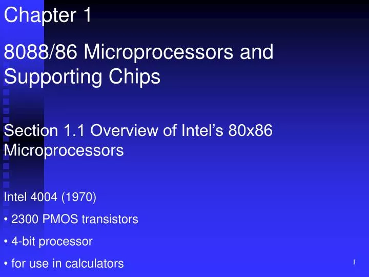
Chapter 1 8088/86 Microprocessors and Supporting Chips Section 1.1 Overview of Intel’s 80x86 Microprocessors Intel 4004 (1970) 2300 PMOS transistors 4-bit processor for use in calculators. PC, terminals for the main frame? No more than 100,000? PCXT, PCAT, …. 586 and Pentium?

E N D
Chapter 1 • 8088/86 Microprocessors and Supporting Chips • Section 1.1 Overview of Intel’s 80x86 Microprocessors • Intel 4004 (1970) • 2300 PMOS transistors • 4-bit processor • for use in calculators
PC, terminals for the main frame? No more than 100,000? PCXT, PCAT, …
586 and Pentium? Pentium MMX series, Pentium II, Pentium III, …
286: virtual memory to 1GB 386: memory to 4GB both physical and virtual memory 486: 80387, 8KB cache memory (data and code mixed) (L1 cache) Pentium: 8KB dada cache, 8K code cache (L1 cache) L2 cache can be 128KB, 256KB, … MMX instructions Multimedia era?
Data Bus 8088: AD0~AD7 8086: AD0~AD15 Address Bus (24pins) 8088: AD0~AD7, A8~A19 8086: AD0~AD15, A16~A19 AD means address and data are commonly used and separated by mux. ALE: Address Latch Enable to latch address signals
Pin Description • BHE (bus high enable): to distinguish between the low byte and high byte of data. • NMI (nonmaskable interrupt), edge-triggered • INTR (interrupt request), active high level triggered • CLOCK, need accurate clock signals • RESET: after reset • READY: insert wait state • Test input from 8087 • What is 8087?
Minimum/Maximum Mode • MN/MX (pin 33) =5V to define pin 24 to pin 31 • Used for the 8085 series
Pins 24-31 in maximum mode QS0 and QS1 (queue status, pins 24 and 25) S0, S1, and S2 (Status signals, pins 26, 27, and 28)
LOCK (pin 29) Used with “LOCK” prefix in the instruction to gain the control of the system bus (prevent DMA to control the bus when the instruction is under processing). LOCK MOV AX, Data RQ/GT0, RQ/GT1 (request/grant, pins 30, 31) These bidirectional pins allow another processor to gain control of the local bus. Pins 24-31 in Minimum Mode
Section 1.3 8284 Clock Generator and Driver • Input pins: • RES (reset in) • X1 and X2 (crystal in): must be three times the desired frequency. IBM PC is 14.31818MHz • F/C (frequency/clock select), select either the crystal input freq or EFI freq • EFI (external frequency in) • CSYNC (clock synchronization), allow several 8284 connected together • RDY1 and AEN1, used as READY signal for inserting WAIT state.
RDY2 and AEN2, like RDY1 and AEN1 and are used for multiprocessing system. • ASYNC • Output signals • RESET • OSC (oscillator), provides the same frequency as the oscillator. • CLK (clock), 1/3 of the crystal frequency and 33% duty cycle • LCLOCK (peripheral clock), 1/2 CLK frequency, 50% duty cycle • READY, for inserting WAIT cycle • Duty cycle?
Input Signals • S0, S1, S2 (status input) • CLK (clock), from 8284 • AEN (address enable) • CEN (command enable) • IOB (input/output bus mode) • Output Signals • MRDC (memory read command) • MWTC (memory write command) • AMWC (advanced memory write) • IORC (I/O read command)
IOWC (I/O write command) • AIOWC (advanced I/O write command) • INTA (interrupt acknowledge) • DT/R (data transmit/receive) • DEN (data enable) • MCE/PDEN (master cascade enable/peripheral data enable) • ALE (address latch enable)
Address bus: 74ls373 (latch) AEN ALE Data bus: DT/R DEN Control Bus: IOR, IOW, MEMR, MEMW
Local bus vs. System bus (refer to Fig. 1-11) IBM PC XT Motherboard Data Flow is shown in pp. 36 of the text book.