Download
1 / 18
180 likes | 347 Views
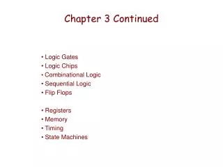
Chapter 3 Continued. Logic Gates Logic Chips Combinational Logic Timing Sequential Logic Flip Flops Registers Memory State Machines. Logical Completeness. Can implement ANY truth table with AND, OR, NOT. 1. AND combinations that yield a "1" in the truth table.

E N D
Chapter 3 Continued Logic Gates Logic Chips Combinational Logic Timing Sequential Logic Flip Flops Registers Memory State Machines
Logical Completeness • Can implement ANY truth table with AND, OR, NOT. 1. AND combinations that yield a "1" in the truth table. 2. OR the resultsof the AND gates. • ALSO: • Can implement ANY truth table with ONLY NANDS. • Can implement ANY truth table with ONLY NORS.
4 Bit Full Adder 1 bit adder 4 bit adder How many gate delays will it take before all of the outputs are correct?
Programmable Logic Arrays (PLAs) • Any combinational logic function can be realized as a sum of products. • Idea: Build a large AND-OR array with lots of inputs and product terms, and programmable connections. • n inputs • AND gates have 2n inputs -- true and complement of each variable. • m outputs, driven by large OR gates • Each AND gate is programmably connected to each output’s OR gate. • p AND gates (p<<2n) • designation is n x m, p ANDs
Example: 4x3 PLA, 6 product terms--- X locates a fuse that can disconnect a line
Example: PAL16L8 Programmable Array Logic (PALs) • How beneficial is product sharing? • Not enough to justify the extra fuse array • PALs ==> fixed OR array • Each AND gate is permanently connected to a certain OR gate.
10 primary inputs • 8 outputs, with 7 ANDs per output • 1 AND for 3-state enable • 6 outputs available as inputs • more inputs, at expense of outputs • two-pass logic, helper terms • Note inversion on outputs • output is complement of sum-of-products • newer PALs have selectable inversion
Designing with PLAs • Compare number of inputs and outputs of the problem with available resources in the PAL • Write equations for each output using programming language like ABEL (Xilinx) Note: VHDL and Verilog are popular computer hardware design languages. ABEL is primarily used for specifying Programmed Logic.
Basic SR Flip Flop Nor Gates: S R | Qn+1 0 0 | Qn 0 1 | 0 1 0 | 1 1 1 | Indeterminate a 1 on S or R sets/resets the FF Nand Gates: S R | Qn+1 0 0 | Indeterminate 0 1 | 1 1 0 | 0 1 1 | Qn a 0 on S or R sets/resets the FF
Clocked SR Flip Flop S R | Qn+1 0 0 | Qn 0 1 | 0 1 0 | 1 1 1 | Indeterminate S, R are nominally 0, a 1 on S or R will set/reset the FF AFTER the Clock Pulse
D Flip Flop (D Latch) D | Qn+1 0 | 0 1 | 1
Master Slave Flip Flop Master sets on rising edge of CP, Slave sets on falling edge of CP. (or visa versa depending on the particular Master Slave)
Toggle Flip Flop T | Qn+1 0 | Qn 1 | not Qn Toggles on CP when T =1
JK Flip Flop J K | Qn+1 0 0 | Qn 0 1 | 0 1 0 | 1 1 1 | not Qn
JK as a Universal Flip Flop JK as an SR – use set and pre inputs JK as a Toggle – connect J and K JK as a D – connect NOT J to K