Download
1 / 159
1.59k likes | 1.72k Views
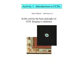
Introduction to CCDs. Basic principles of CCD imaging. Original notes by S.Tulloch & G.Bonanno modified and integrated by GPS (Rev.103 Nov08). What is a CCD ?. Charge Coupled Devices (CCDs) were invented in the 1970s and originally found application as memory devices

E N D
Introduction to CCDs Basic principles of CCD imaging Original notes by S.Tulloch & G.Bonanno modified and integrated by GPS (Rev.103 Nov08)
What is a CCD ? Charge Coupled Devices (CCDs) were invented in the 1970s and originally found application as memory devices and more recently as shift registers, analog delay lines, particle detectors. Their light sensitive properties were quickly exploited for imaging applications (TV cameras) and they produced a major revolution in Astronomy. They improved the light gathering power of telescopes by almost two orders of magnitude. Nowadays an amateur astronomer with a CCD camera and a 15 cm telescope can collect as much light as an astronomer of the 1960s equipped with a photographic plate and a 1m telescope. CCDs work by converting light into a pattern of electronic charge in a silicon chip. This pattern of charge is converted into a video waveform, digitised and stored as an image file on a computer. The sensitive surface of a CCD is composed of a large number of juxtaposed square or rectangular elements (pixels) sensitive to light; each pixel (a few microns size) creates and accumulates electrical charge proportional to the amount of light it has received and constitutes an elementary point of the image, as does each grain of a photographic film. It is the reading of the accumulated charges in the different pixels that allow the image to be reconstructed. CCDs used in astronomy are all black and white detectors; it is possible to produce color images by trichromatism (three images of the same object, each one with one of the three fundamental filters and combine these images during analysis). CCDs have practically no detection threshold (unlike films) and the number of electrons generated gives a direct photometric measure.
Il rumore intrinseco di un rivelatore e’ tutto ciò che e’ introdotto dal rivelatore stesso e non dal segnale. Determina la soglia inferiore di rilevabilità (con basso rumore intrinseco si osservano sorgenti più deboli) • Il rumore di un CCD e’ dovuto a: • Agitazione termica (trascurabile al di sotto di -100°C • Rumore di lettura del circuito di uscita (ineliminabile) Se il rivelatore non introducesse rumore, l’unico a restare sarebbe quello della sorgente stessa (RSHOT = √Nfotoni). • Per fare analisi quantitative il segnale deve superare di almeno 3 volte il rumore • Il minimo valore di segnale misurabile e’ detto “sensibilità” e si può considerare dato dal rumore del rivelatore • “Dynamic range”: the ratio, usually expressed in decibels, of the maximum to the minimum signal that a system can handle (Grey levels). Used to describe the limits of receivers.
Hole Electron Photoelectric Effect The effect is fundamental to the operation of a CCD. Atoms in a silicon crystal have electrons arranged in discrete energy bands. The lower energy band is called the Valence Band, the upper band is the Conduction Band. Most of the electrons occupy the Valence band but can be excited into the conduction band by heating or by the absorption of a photon. The energy required for this transition is 1.26 electron volts (eV). Once in this conduction band the electron is free to move about in the lattice of the silicon crystal. It leaves behind a ‘hole’ in the valence band which acts like a positively charged carrier. In the absence of an external electric field the hole and electron will quickly re-combine and be lost. In a CCD an electric field is introduced to sweep these charge carriers apart and prevent recombination. photon photon Conduction Band Increasing energy 1.26eV Valence Band Thermally generated electrons are indistinguishable from photo-generated electrons . They constitute a noise source known as ‘Dark Current’ and it is important that CCDs are kept cold to reduce their number. 1.26eV corresponds to the energy of light with a wavelength of 1mm. Beyond this wavelength silicon becomes transparent and CCDs constructed from silicon become insensitive.
CCD Analogy A common analogy for the operation of a CCD is as follows: An number of buckets (Pixels) are distributed across a field (Focal Plane of a telescope) in a square array. The buckets are placed on top of a series of parallel conveyor belts and collect rain fall (Photons) across the field. The conveyor belts are initially stationary, while the rain slowly fills the buckets (During the course of the exposure). Once the rain stops (The camera shutter closes) the conveyor belts start turning and transfer the buckets of rain , one by one , to a measuring cylinder (Electronic Amplifier) at the corner of the field (at the corner of the CCD) The animation in the following slides demonstrates how the conveyor belts work.
CCD Analogy CCD COLUMNS (VERTICAL CONVEYOR BELTS) PHOTONS PIXELS (BUCKETS) OUTPUT AMPLIFIER SERIAL REGISTER(HORIZONTAL CONVEYOR BELT)
Exposure finished, buckets now contain samples of rain, i.e. charge has been collected in pixels.
Conveyor belt starts turning and transfers buckets. Rain collected on the vertical conveyor is tipped into buckets on the horizontal conveyor. SERIAL REGISTER(HORIZONTAL CONVEYOR BELT)
Vertical conveyor stops. Horizontal conveyor starts up and tips each bucket in turn into the measuring cylinder .
After each bucket has been measured, the measuring cylinder is emptied , ready for the next bucket load. ` OUTPUT AMPLIFIER
A new set of empty buckets is set up on the horizontal conveyor and the process is repeated.
Eventually all the pixels have been measured, the CCD has been read out.
CCD main functions Exposure 1. Charge generation: photoelectric effect 2. Charge collection: potential walls (pixels) Shutter closes 3. Charge transfer: CCD columns shift 4. Readout: serial register and amplification
Structure of a CCD 1. The image area of the CCD is positioned at the focal plane of the telescope. An image then builds up that consists of a pattern of electric charge. At the end of the exposure this pattern is then transferred, pixel by pixel, through the serial register to the on-chip amplifier. Electrical connections are made to the outside world via a series of bond pads and thin gold wires positioned around the chip periphery. Image area Metal, ceramic or plastic package • CCD: 512x512 pixels, 1024x1024, 2048x2048, 4096x4096 • Sensitive surface: • TC211: 2.64x2.64mm2 • (192x165 pixels, 13.75x16µm size) • Thomson 7863: 8.8x6.6mm2 • (384x288 pixels, 23x23µm) • SITe SI-003A: 24.6x24.6mm2 • (1024x1024 pixels, 24x24µm) • LORAL 2K3eb: 30.7x30.7mm2 • (2048x2048 pixels, 15x15µm) • CCD arrays may be smaller in comparison with standard photography (24x36mm). “Buttable” CCDs for mosaic. Connection pins Gold bond wires Bond pads Silicon chip On-chip amplifier Serial register
Structure of a CCD 2. CCDs are are manufactured on silicon wafers using the same photo-lithographic techniques used to manufacture computer chips. Scientific CCDs are very big ,only a few can be fitted onto a wafer. This is one reason that they are so costly. The photo below shows a silicon wafer with three large CCDs and assorted smaller devices. A CCD has been produced by Philips that fills an entire 6 inch wafer! It is the worlds largest integrated circuit. Don Groom LBNL
Structure of a CCD 3. The diagram shows a small section (a few pixels) of the image area of a CCD. This pattern is reapeated. Channel stops to define the columns of the image Plan View Transparent horizontal electrodes to define the pixels vertically. Also used to transfer the charge during readout One pixel Electrode Insulating oxide n-type silicon p-type silicon Cross section Every third electrode is connected together. Bus wires running down the edge of the chip make the connection. The channel stops are formed from high concentrations of Boron in the silicon.
Structure of a CCD 4. Below the image area (the area containing the horizontal electrodes) is the ‘Serial register’ . This also consists of a group of small surface electrodes. There are three electrodes for every column of the image area. Image Area On-chip amplifier at end of the serial register Serial Register Cross section of serial register Once again every third electrode in the serial register is connected together.
Structure of a CCD 5. 160mm Details of a corner of an EEV CCD Image Area Serial Register Bus wires Edge of Silicon Read Out Amplifier The serial register is bent twice to move the output amplifier away from the edge of the chip (Voltage bus). The arrows indicate how charge is transferred through the device.
R R Structure of a CCD 6. Details of the on-chip amplifier of a Tektronix CCD and its circuit diagram Output Drain (OD) 20mm Gate of Output Transistor SW RD OD Output Source (OS) Output Node Reset Transistor Reset Drain (RD) Summing Well Output Node Output Transistor Serial Register Electrodes OS Summing Well (SW) Substrate Last few electrodes in Serial Register
n p Electric Field in a CCD 1. The n-type layer contains an excess of electrons that diffuse into the p-layer. The p-layer contains an excess of holes that diffuse into the n-layer. This structure is identical to that of a diode junction. The diffusion creates a charge imbalance and induces an internal electric field. The electric potential reaches a maximum just inside the n-layer, and it is here that any photo-generated electrons will collect. All science CCDs have this junction structure, known as a ‘Buried Channel’. It has the advantage of keeping the photo-electrons confined away from the surface of the CCD where they could become trapped. It also reduces the amount of thermally generated noise (dark current). Electric potential Electric potential Potential along this line shown in graph above. Cross section through the thickness of the CCD
Electric Field in a CCD 2. During integration of the image, one of the electrodes in each pixel is held at a positive potential. This further increases the potential in the silicon below that electrode and it is here that the photoelectrons are accumulated. The neighboring electrodes, with their lower potentials, act as potential barriers that define the vertical boundaries of the pixel. The horizontal boundaries are defined by the channel stops. Electric potential Region of maximum potential n p
p-type silicon n-type silicon Charge Collection in a CCD. Photons entering the CCD create electron-hole pairs. The electrons are then attracted towards the most positive potential in the device where they create ‘charge packets’. Each packet corresponds to one pixel pixel boundary pixel boundary incoming photons Electrode Structure Charge packet SiO2 Insulating layer
1 2 3 Charge Transfer in a CCD 1. In the following few slides, the implementation of the ‘conveyor belts’ as actual electronic structures is explained. The charge is moved along these conveyor belts by modulating the voltages on the electrodes positioned on the surface of the CCD. In the following illustrations, red electrodes are held at a positive potential, black ones are held at a negative potential.
1 2 1 2 3 3 Charge Transfer in a CCD 2. +5V 0V -5V +5V 0V -5V +5V 0V -5V Time-slice shown in diagram
1 2 1 2 3 3 Charge Transfer in a CCD 3. +5V 0V -5V +5V 0V -5V +5V 0V -5V