Download
1 / 24
240 likes | 408 Views
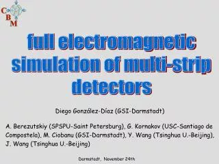
9th Topical Seminar on Innovative Particle and Radiation Detectors May 23-26, 2004- Siena, Italy. A full Monte Carlo simulation code for silicon strip detectors. M. Brigida, C. Favuzzi, P. Fusco, F. Gargano, N. Giglietto, F. Giordano, F. Loparco ,

E N D
9th Topical Seminar on Innovative Particle and Radiation Detectors May 23-26, 2004- Siena, Italy A full Monte Carlo simulation code for silicon strip detectors M. Brigida, C. Favuzzi, P. Fusco, F. Gargano, N. Giglietto, F. Giordano, F. Loparco, B. Marangelli, M. N. Mazziotta, N. Mirizzi, S. Rainò, P. Spinelli Bari University & INFN
The simulation chain Charged particles Photons Interaction with silicon Ionization energy loss Photoelectric absorption Primary e-h pairs Secondary e-h pairs Drift of charge carriers Electronics simulation Electronic noise Voltage signals on the readout strips Induced current signals Electronics chain Propagation of carriers
Energy loss of charged particles in silicon L-shells (~150 eV) M-shell (~17 eV) The energy loss in Si is evaluated from the collision cross section σ(E) (H. Bichsel, Rev. Mod. Phys. 60, 663) K-shell (~1850 eV) The number of collisions per unit path length is evaluated as:
Generation of e-h pairs in silicon Ionizing particle Virtual γ Si atom Primary e-h pairs Phonon scattering Secondary e-h pairs
Silicon energy levels Conduction band Energy gap Eg = 1.12 eV @T=300K Valence band EV= [-12, 0] eV Energy L-shells EL2-3= -99.2 eV EL1= -148.7 eV K-shell Ek= -1839 eV
Generation of e-h pairs • Primary carriers: are produced in the primary collisions of the incident particle with the silicon absorber, with the absorption of virtual photons by the medium. • Secondary carriers: are produced by the subsequent energy losses of primary (and secondary) carriers. The relative absorption probabilities depend on the photon energy. For energies above the K-shell there is a 92% probability of absorption by the K-shell and an 8% probability of absorption by the L1-shell
Primary e-h pairs • Absorption by an inner shell (x=K, L1, L23): • A hole is left in the shell with energy Eh=Ex • A photoelectron is ejected with energy Epe=E-Ex-Egap • Absorption by the valence band (M shell): • A hole is left with an energy Eh random distributed in the range [0,EV] (EV=12eV) • A photoelectron is ejected with energy Epe=E-Eh-Egap • The relaxation process following photon absorption yields electrons and vacancies in the K, L1 and L23 shells.
Silicon shells relaxation trees Electron and hole energies are assigned according to Sholze et al, J. Appl. Phys. 84 (1998), 2926
Production of secondary e-h pairs A primary electron (hole) with E > Ethr (Ethr=3/2 Egap) can interact with the Si absorber by ionization or by phonon scattering. The ratio between the ionization rate and the phonon scattering rate is: where A=5.2 eV3 and E0is the phonon energy (E0=63 meV @ T=300 K) The generation of secondary pairs is a cascade process, that is simulated with a MC method. At the end of each step, a carrier can emit a phonon or can cause ionization. In this case a new e-h pair is created.
Pair creation energy & Fano factor Pairs generated by photons Pairs generated by electrons (holes) The pair creation energy approaches the value W∞=3.645 eV for large primary energies The Fano Factor approaches the limit F∞=0.117 for large primary energies
Pair distribution along the track βγ=5 electron tracks in 400 m silicon
p+ strips h w p d n bulk SSD geometry The p strips are grounded, the back is kept at a positive voltage V0 • "Small pitch" geometry: • d=325 m, p=25 m • w=12 m, h=5m • V0=100 V • "Large pitch" geometry: • d=400 m, p=228 m • w=60 m, h=5m • V0=100 V
The electric field "Large pitch" configuration The electric field has been calculated by solving the Maxwell equation: in an elementary detector cell with the following boundary conditions for the potential: The calculation has been performed using the ANSOFT MAXWELL 2D field calculator.
Motion of charge carriers After being produced, electrons and holes will drift under the action of the electric field towards the n back and the p strips, according to the equation: where the mobility is related to the E field by the parameterization: The parameters vm, β and Ec are different for electron and holes and depend on the temperature. During their drift, carriers are diffused by multiple collisions according to a gaussian law:
Induced current signals The current signals induced by the moving carriers on the readout electrodes (p strips) are calculated using the Shockley-Ramo's theorem: The weighting field Ekdescribes the geometrical coupling between the moving carrier and the k-th electrode. It has been evaluated by solving the same Maxwell's equation as for the electric field with ρ=0 and with the boundary conditions:
Weighting potential Readout strip "Large pitch" configuration Back electrode Adjacent strips
Simulation of the electronics Front-end electronics H(s) Input current signal i(t) Output voltage signal V(t) The transfer function can be expressed as a ratio of polynomials The output signals are evaluated in the time domain by solving the inverse Laplace transform with the finite difference approximation for the time derivatives Noise contributions are added by taking into account the proper noise transfer functions
Front-end electronics Detector Preamplifier Shaper
Noise simulation The electronic noise is due to the detector and to the electronic front-end. Thermal noise due to the feedback resistor: i2nf=4KT/Rf Electronic noise due to the amplifier: i2na= 0 v2na = 2.7KT/gm Shot noise due to the leakage current: i2nd=2eIL Thermal noise due to the bias resistor: i2nb=4KT/Rb
Charge sharing analysis (1) To study the charge sharing a sample of MIPs has been simulated, crossing the detector with null zenith angle, in the region between two strips The charge sharing has been studied with the η function:
Charge sharing analysis (2) • Both the η distribution are symmetric around the value η=0.5 • In the large pitch geometry the peaks are located at η≈0 and η≈1 → weak coupling between adjacent strips • In the small pitch geometry the peaks are located at η≈0.2 and η≈0.8→ strong coupling between adjacent strips
Comparison with experimental data • A beam test has been carried out exposing a 400m thick SSD with 228m strip pitch to a 3 GeV/c π beam @ CERN-PS T9 beam facility • Experimental data are in good agreement with the MC prediction
Conclusions • We have developed a new MC full simulation code that includes all the physical processes taking place in a SSD • The MC code can be used with different detector geometries and front-end electronics • The temperature dependence of the physical processes is taken into account, thus allowing a study of the SSD performance with the temperature (an example will be given in S. Rainò's talk) • A charge sharing analysis has been performed, showing that the MC predictions are in good agreement with experimental data • Our MC code allows to study the efficiency and the space resolution of SSDs (an example will be shown in M. Brigida's talk) • For further details: http://www.ba.infn.it/~mazziot/article.pdf