Download
1 / 22
290 likes | 871 Views
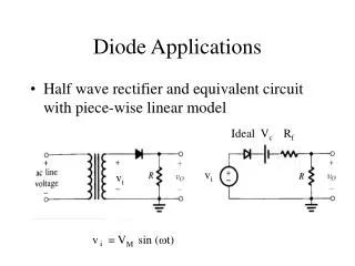
Lecture 8 Diode Applications and small signal models. 1. Agenda. -Diode Regulator -Zener Diode -Design of regulator circuits -Clamping circuits (DC-restoration) -Diode Small Signal Models. 2. Application 2: Voltage Regulators: Introduction to Reverse Breakdown.

E N D
Agenda -Diode Regulator -Zener Diode -Design of regulator circuits-Clamping circuits (DC-restoration)-Diode Small Signal Models 2
Application 2: Voltage Regulators:Introduction to Reverse Breakdown Increased reverse bias eventually results in the diode entering the breakdown region, resulting in a sharp increase in the diode current. The voltage at which this occurs is the breakdown voltage, VZ. 2 V < VZ< 2000 V 3
Reverse Breakdown Mechanisms • Zener BreakdownZener breakdown occurs in heavily doped diodes. The heavy doping results in a very narrow depletion region at the diode junction. Reverse bias leads to carriers with sufficient energy to tunnel directly between conduction and valence bands moving across the junction. Once the tunneling threshold is reached, additional reverse bias leads to a rapidly increasing reverse current. 4
Knee Current Valid iff IZ > IZK Zener Diode 5
Zener Diode Model In breakdown, the diode is modeled with a voltage source, VZ, and a series resistance, RZ. RZ models the slope of the i-v characteristic. Diodes designed to operate in reverse breakdown are called Zener diodes and use the indicated symbol. 6
Analysis of Zener Diodes Choose 2 points (0V, -4 mA) and (-5 V, -3 mA) to draw the load line.It intersects with i-v characteristic at Q-point (-2.9 mA, -5.2 V). 2.Using piecewise linear model: 1.Using load-line analysis: Since IZ >0 (ID <0), solution is consistent with Zener breakdown assumption. 7
Rectifier Filter 120 Vrms C R Unregulated supply RL Regulator design Less ripple larger C We can get less ripple without using a larger C with a Zener regulator 8
Voltage Regulator using Zener Diodeconstant voltage model For proper regulation, Zener current must be positive. If Zener current <0, Zener diode no longer controls voltage across load resistor and voltage regulator is said to have “dropped out of regulation”. Zener diode keeps voltage across load resistor constant. For Zener breakdown operation, IZ >0. 9
Voltage Regulator using Zener Diode: Example (Including Zener Resistance) Problem: Find output voltage and Zener diode current for Zener diode regulator. Given data: VS=20 V, R=5 kW, RZ=0.1 kW, VZ=5 V Analysis: Output voltage is a function of current through Zener diode. 10
Rth R IL + rZ + VZo Regulator Characteristics Thevenin Equivalent VOC For best regulation rZ <<<< limitation on the value of Iz Line Regulation Load regulation 11
Line and Load Regulation Line regulation characterizes how sensitive output voltage is to input voltage changes. Line Regulation mV/V For fixed load current, Line regulation = Load regulation characterizes how sensitive output voltage is to changes in load current withdrawn from regulator. Load Regulation Ohms For changes in load current, Load regulation = Load regulation is Thevenin equivalent resistance looking back into regulator from load terminals. 12
R IL IZ + rZ VZo Selecting R to keep Zener Diode in the Breakdown Region 13
Application 3: Peak Detector Circuit(Clamping circuit) As input voltage rises, diode is on and capacitor (initially discharged) charges up to input voltage minus the diode voltage drop. At peak of input, diode current tries to reverse, diode cuts off, capacitor has no discharge path and retains constant voltage providing constant output voltage Vdc = VP – Vd,on. 14
Application 4: Clipping or Limiting Circuits Clipping circuits have dc path between input and output, whereas clamping circuits use capacitive coupling between input and output. The voltage transfer characteristic shows that gain is unity for vI < VC, and gain is zero for vI > VC. A second clipping level can also be set or diodes can be used to control circuit gain by switching resistors in and out of circuits. 15
Clamping or DC-Restoring Circuit After the initial transient lasting less than one cycle in both circuits, output waveform is an undistorted replica of input. Both waveforms are clamped to zero. Their dc levels are said to be restored by the clamping circuit. Clamping level can also be shifted away from zero by adding a voltage source in series with diode. 16