Download
1 / 1
10 likes | 108 Views
CNMS Staff Science Highlight. High Purity Direct-Write Nanoscale Fabrication. Scientific Achievement

E N D
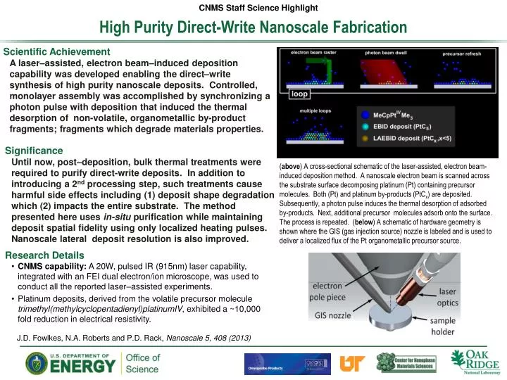
CNMS Staff Science Highlight High Purity Direct-Write Nanoscale Fabrication • Scientific Achievement • A laser–assisted, electron beam–induced deposition capability was developed enabling the direct–write synthesis of high purity nanoscale deposits. Controlled, monolayer assembly was accomplished by synchronizing a photon pulse with deposition that induced the thermal desorption of non-volatile, organometallic by-product fragments; fragments which degrade materials properties. #6 1.5 nm #4 1.1 nm #5 1.4 nm #3 1.1 nm #1 0.83 nm #2 0.96 nm • Significance • Until now, post–deposition, bulk thermal treatments were required to purify direct-write deposits. In addition to introducing a 2nd processing step, such treatments cause harmful side effects including (1) deposit shape degradation which (2) impacts the entire substrate. The method presented here uses in-situ purification while maintaining deposit spatial fidelity using only localized heating pulses. Nanoscale lateral deposit resolution is also improved. (above) A cross-sectional schematic of the laser-assisted, electron beam-induced deposition method. A nanoscale electron beam is scanned across the substrate surface decomposing platinum (Pt) containing precursor molecules. Both (Pt) and platinum by-products (PtCx) are deposited. Subsequently, a photon pulse induces the thermal desorption of adsorbed by-products. Next, additional precursor molecules adsorb onto the surface. The process is repeated. (below) A schematic of hardware geometry is shown where the GIS (gas injection source) nozzle is labeled and is used to deliver a localized flux of the Pt organometallic precursor source. • Research Details • CNMS capability: A 20W, pulsed IR (915nm) laser capability, integrated with an FEI dual electron/ion microscope, was used to conduct all the reported laser–assisted experiments. • Platinum deposits, derived from the volatile precursor molecule trimethyl(methylcyclopentadienyl)platinumIV, exhibited a ~10,000 fold reduction in electrical resistivity. J.D. Fowlkes, N.A. Roberts and P.D. Rack, Nanoscale 5, 408 (2013)