Download
1 / 97
1.01k likes | 1.37k Views
Design at the Register Transfer Level. Chapter 8. 8-1 Introduction. A digital system is a sequential logic system constructed with flip-flops and gates. To specify a large digital system with a state table is very difficult . Modular subsystems

E N D
Design at the Register Transfer Level Chapter 8
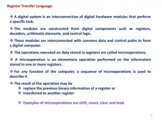
8-1 Introduction • A digital system is a sequential logic system constructed with flip-flops and gates. • To specify a large digital system with a state table is very difficult . • Modular subsystems • Registers, decoders, multiplexers, arithmetic elements and control logic. • They are interconnected with datapaths and control signals.
8-2 Register Transfer Level (RTL) Notation • A digital system is represented at the register transfer level (RTL) when it is specified by the following three components: • The set of registers in the system. • The operations that are performed on the data stored in the registers. • The control that supervises the sequence of operations in the system.
The statement R2← R1 denotes a transfer of the contents of register R1 into register R2. A conditional statement governing a register transfer operation is symbolized with an if-then statement such as If (T1 =1)then (R2← R1) where T1 is a control signal generated in the control section.
Other example: R1← R1 + R2 Add contents of R2 to R1 R3← R3 + 1 Increment R3 by 1 R4← shr R4 Shift right R4 R5← 0 Clear R5 to 0
The type of operations most often encountered in digital system: • Transfer operations, which transfer data from one register to anther. • Arithmetic operations, which perform arithmetic on data in registers. • Logic operations, which perform bit manipulation of nonnumeric data in registers. • Shift operations, which shift data between registers.
8-3 Register Transfer Level in HDL • Example (a) assign S = A + B; //continuous assignment for addition operation (b) always @ (A, B) //level-sensitive cyclic behavior S = A + B; //combinational logic for addition operation (c) always @ (negedge clock) //edge-sensitive cyclic behavior begin RA = RA + RB; //blocking procedural assignment for addition RD = RA; //register transfer operation end (d) always @ (negedge clock) //edge-sensitive cyclic behavior begin RA < =RA + RB; //nonblocking procedural assignment for addition RD < =RA; //register transfe operation end
Example: If A =1010, B =0000,then A has the Boolean value 1, B has Boolean value 0. Results of other operation with these value: A && B =0 //logical AND A | | B =1 //logical OR ! A =0 //logical complement ! B =1 //logical complement (A > B)=1 //is greater than (A == B)=0 //identity (equality)
The relational operators === and ! ==test for bitwise (identity) and inequality in Verilog' s four-valued logical system. • Example: If A =0xx0, B =0xx0,then A ===B =1, but A == B would evaluate to x. • Other example: If R =11010, then R = R >> 1, the value R is 01101. R = R >>> 1, the value R is 11101. If R =01101, then R = R >>> 1, the value R is 00110.
Loop Statement ■ repeat loop ■ forever loop initial initial begin begin clock =1'b0; clock =1'b0; repeat (16) forever #5 clock =~clock; #10 clock =~clock; end end ■ while loop ■ for loop integer count; for (j =0; j < 8; j = j + 1) initialbegin begin //procedural statement go here count =0; end while (count < 64) #5 clock = count + 1; end
Logic Synthesis • A statement with a conditional operator such as assign Y = S ? In_1 : In_0; translates into a two-to-one-line multiplexer with control input S and data input In_1 and In_0. • A cyclic behavior (always ...)may imply a combinational or sequential circuit, depending on whether the event control expression is level sensitive or edge sensitive.
always @ (In_1 or In_0 or S) if (S) Y = In _ 1; else Y = In _ 0; translates into a two-to-one-line multiplexer. An edge-sensitive cyclic behavior (e.g., always @ (posedge clock)) specifies a synchronous (clocked) sequential circuit. Examples of such circuits are registers and counters.
FIGURE 8.1 A simplified flowchart for HDL-based modeling, verification, and synthesis
8.4Algorithmic State Machines (ASMs) • The logic design of digital system can be divided into two distinct parts. • One is concerned with the design of the digital circuits that perform the data-processing operations. • The other is concerned with the design of the control circuits that determine the sequence in which t he various actions are performed.
The control logic that generates the singles for sequencing the operations in the data path unit is a finite state machine (FSM). • The control sequence and datapath tasks of the digital system are specified by means of a hardware algorithm. It solved the problem with a given piece of equipment. • A flowchart that has been developed specifically to define digital hardware algorithm is called an al gorithmic state machine (ASM) chart.
ASM Chart • The ASM chart is composed of three basic elements: • State box • Decision box • Conditional box • They connected by directed edges indicating the sequential precedence and evolution of the states as the machine operates.
FIGURE 8.3 ASM chart state box FIGURE 8.4 ASM chart decision box
ASM block FIGURE 8.6 ASM block
Simplifications FIGURE 8.7 State diagram equivalent to the ASM chart of Fig. 8.6
Timing Considerations • The timing for all register and flip-flop in digital system is controlled by a master-clock generator. FIGURE 8.8 Transition between states
ASMD Chart • Contrasted between Algorithmic State Machine and Datapath (ASMD) charts & ASM charts. • An ASMD chart are does not list register operations within a state box. • The edges of an ASMD charts are annotated with register operations that are concurrent with the state transition indicated by the edge. • An ASMD chart includes conditional boxes identifying the singles which control the register operation s that annotate the edges of the chart. • An ASMD chart associates register operations with state transitions rather than with state.
Designed an ASMD chart have three-step: • Form an ASM chart displaying only how the inputs to the controller determine its state transitions. • Convert the ASM chart to an ASMD chart by annotating the edges of ASM chart to indicate to the concur rent register operations of the datapath unit. • Modify the ASMD chart to identify the control singles that are generated by the controller and the ca use the indicated register operations in the datapath unit.
8.5 Design Example FIGURE 8.9 (a) Block diagram for design example
FIGURE 8.9 (b) ASMD chart for controller state transitions, asynchronous reset (c)ASMD chart for controller state transitions, synchronous reset (d)ASMD chart for a completely specified controller, asynchronous reset
FIGURE 8.11 Register transfer-level description of design example
The D input of flip-flip G1 must be equal to 1 during present state S_1 when both inputs A2 and A3 are equal to 1. This condition is expressed with the D flip-flop input equation DG1 = S_1 A2 A3 Similarly, the next-state column of G0 has four 1' s, and the condition for setting this flip-flop is DG0 = Start S_idle + S_1 To derive the five output function, we can exploit the fact that state 10 is not used, which simplifies the equation for clr_A_F and enables us to obtain the following simplified set of output equations:
set_E = S_1 A2 clr_E = S_1 A2' set_F = S_2 clr_A_F = Start S_idle incr_A = S_1 The logic diagram showing the internal detail of the controller of Fig. 8.10 is drawn in Fig. 8.12.
8.6 HDL Description of Design Example • Structural • The lowest and most detailed level • Specified in terms of physical components and their interconnection • RTL • Imply a certain hardware configuration • Specified in terms of the registers, operations performed, and control that sequences the operations. • Algorithmic-based behavioral • The most abstract • Most appropriate for simulating complex to verify design ideas and explore tradeoffs
The manual method of design developed • A block diagram (Fig. 8.9(a)) shoeing the interface between the datapath and the controller. • An ASMD chart for the system. (Fig. 8.9(d)) • The logic equations for the inputs to the flip-flops of the controller. • A circuit that implements the controller (Fig. 8.12). • In contrast, an RTL model describes the state transitions of the controller and the operations of the datapath as a step towards automatically synthesizing the circuit that implements them.
Structural Description • HDL example 8.4 presents the structural description of the design example. It consists of a nested hierarchy of modules and gates describing: • The top-level module, Design_example_STR • The modules describing the controller and the datapath • The modules describing the flip-flops and counters • Gates implementing the logic of controller
The top-level module (see Fig. 8.10) encapsulates the entire design by: • Instantiating the controller and the datapath modules • Declaring the primary (external) input signals • Declaring the output signals • Declaring the control signals generated by the controller and connected to the datapath unit • Declaring the status signals generated by the datapath unit and connected to the controller