Download
1 / 1
10 likes | 118 Views
Empirical Molecular Dynamics Simulations to Analyse Holographically Determined Mean Inner Potentials. Si.95Ge.05. Si.75Ge.25. Si.5Ge.5. Si.25Ge.75. Si.05Ge.95. a. b. j. i. 2. 1. j. j. potential scan. Vacuum. k. Ge-Si. j. i. y. c. k. i. x. Si substrate. V 0. t. Object.

E N D
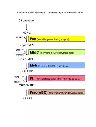
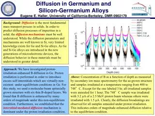
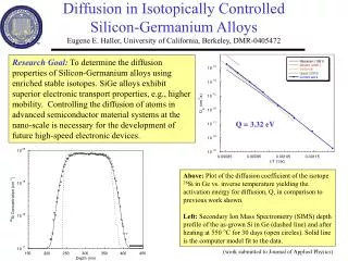
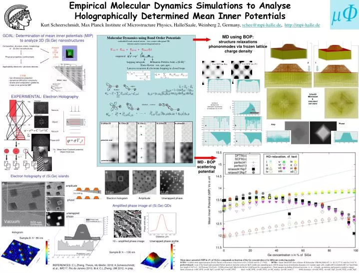
Empirical Molecular Dynamics Simulations to Analyse Holographically Determined Mean Inner Potentials Si.95Ge.05 Si.75Ge.25 Si.5Ge.5 Si.25Ge.75 Si.05Ge.95 a b j i 2 1 j j potential scan Vacuum k Ge-Si j i y c k i x Si substrate V0 t Object i d j potential average SiGeQD MDrelaxed & simulated exit wave Vacuum Si.5Ge.5 background histogram (counts/eV) & linescans (Vo in eV) angles -4eV Phase shift distance l k V0: Mean inner Coulomb potential t: Object thickness a b Phase i Amp dihedral ,,,, torsion c d + + ...... + = Kurt Scheerschmidt, Max Planck Institute of Microstructure Physics, Halle/Saale, Weinberg 2, Germany, schee@mpi-halle.de, http://mpi-halle.de GOAL: Determination of mean inner potentials (MIP) to analyze 3D (Si,Ge) nanostructures MD using BOP: structure relaxations phononmodes via frozen lattice charge density Molecular Dynamics using Bond Order Potentials embedded bonds instead atoms – two-center orthogonal TB density matrix instead diagonalisation Composition, structure, strain, morphology of (Si,Ge) nanostructures Analysis via STEM & CTEM E tot = Erep + Eprom + Eband (k) empirical s2p2->sp3SHia,jbQia,jb Physical properties (confinement) hopping integrals BOmatrix Pettifor-Aoki = [E-H]-1 Slater-Koster sss, sps, ppp... Lanczos recursion & electronic hopping in closed loops V(r)BOP (in eV) V(r) DFT (in Ha) Applicability electronic / photonic devices • CTEM: • - two dimensional projection • - dynamical diffraction complexity • strains and composition gradients • mean inner potential MIP EXPERIMENTAL: Electron Holography y ~ eiAt = C-1{eigt}C MD - BOP scattering potential Electron holography of (Si,Ge) islands amplitude Si Ion milling Electron hologram Amplitude Unwrapped phase phase Amplified phase image of (Si,Ge) QDs unwrapped phase Hologram Sample A: h~ 66 nm 10 amplified phase image Unwrapped phase profile Sample B: h ~ 130 nm Mean inner potential (MIP in eV) of (Si,Ge) compounds as function of the Ge concentration x for different scattering models: SCFfit = isolated atom approximation (Doyle-Turner) with atomic form factor of Si (5.828Å) and Ge (7.378Å). - DFTfit = linear fitted DFT data of Kruse & Schowalter UM106(2006)105, i.e. Si (12.57 V) and Ge (14.67 V). perfect/relaxed = scan of the bond order potential before (perfect) and after (relaxed, NpT conditions) annealing up to 400 K using classical molecular dynamics for vacuum super cells (small=sSC/extended=eSC) of 7nm/23nm box length (13x13x13, 10478atoms/ 41x41x41, 312666 atoms) half filled with (Si,Ge) of different Ge concentration x. Total energies including all attraction terms, i.e. s-, p-bonds , promotion, and negative repulsive energy. Static relaxation: i=sSC,NVE, ii=sSC,NpT, iii=eSC,NpT, iv=eSC,NVE final: v=eSC,NVE, vi=sSC,NVE, xi=sSC,weak-p, xii=sSC,weak-T 400K-dynamics: vii=eSC,NVE, viii=eSC,NpT, ix=sSC,NVE, x=sSC,NpT REFERENCES: C.L.Zheng, Thesis, HU-Berlin, 2010; K.Scheerschmidt, et.al., IMC17, Rio de Janeiro 2010, I8.4; C.L.Zheng, UM 2012, in prep.