Download
1 / 4
70 likes | 116 Views
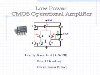
In the electronics industry the Low Power Comparator using High Speed in Analog to Digital Converters. In electronic device Comparator are mostly used in Analog to Digital converter ADC . In ADC are used for the delay produced and power consumed by an ADC. I design a 0.18u00b5-m CMOS Comparator for High Speed Application. The advantage of programmable hysteresis to the comparators are also discussed. Tanner EDA is used for the design and simulation for the comparator circuits The difference between the proposed comparator to the existing double tail comparator result are produced. G. Naveen Balaji | S. Karthikeyan | M. Merlin Asha "0.18u00b5-m CMOS Comparator for High-Speed Applications" Published in International Journal of Trend in Scientific Research and Development (ijtsrd), ISSN: 2456-6470, Volume-1 | Issue-5 , August 2017, URL: https://www.ijtsrd.com/papers/ijtsrd2356.pdf Paper URL: http://www.ijtsrd.com/engineering/electronics-and-communication-engineering/2356/018-u00b5m-cmos-comparator-for-high-speed-applications/g-naveen-balaji<br>

E N D
International Journal of Trend in Scientific Research and Development (IJTSRD) International Open Access Journal ISSN No: 2456 - 6470 | www.ijtsrd.com | Volume - 1 | Issue – 5 0.18µm CMOS Comparator for High-Speed Applications G. Naveen Balaji Assistant Professor, Department of ECE, SNS College of Technology, Coimbatore, India S. Karthikeyan PG Scholar, Department of ECE, SNS College of Technology, Coimbatore, India M. Merlin Asha PG Scholar, Department of ECE, SNS College of Technology, Coimbatore, India ABSTRACT thickness and extent are modify for low power consumption and high operating speed. Hysteresis in the comparator circuit is applied by a small portion of the output voltage to the positive input. Hysteresis relate to the comparator circuit to reduce the circuit reactivity to noise and produce the output if the input in the state will be change slowly. A model for the comparator is designed and output is produced and comparison results are obtained for the proposed model and the existing model. To design the existing model is tanner EDA tool. The research paper is organized as follows: an introduction to CMOS comparator is given and high speed comparator architecture with properties for each structure will be discussed. And last stage is simulation result for all the architecture will be shown and discussed. CIRCUIT DESIGN ANALYSIS The two-stage CMOS amplifier is a first comparator with output inverter has three stages. Differential amplifier is the first stage, common-source amplifier is the second stage, and inverting buffer is the third stage. The input bias current is designed for 1μA. The bias current of the proposed current mirror of two gain stages is 3μA. The two analog input voltages are connected to the differential pair. The reference In the electronics industry the Low Power Comparator using High Speed in Analog to Digital Converters. In electronic device Comparator are mostly used in Analog to Digital converter (ADC). In ADC are used for the delay produced and power consumed by an ADC. I design a 0.18µm CMOS Comparator for High-Speed Application. The advantages of programmable hysteresis to the comparators are also discussed. Tanner EDA is used for the design and simulations for the comparator circuits the difference between the proposed comparator to the existing double tail comparator result are produced. Keyword: Low power Comparator, Analog to digital converter, two stage CMOS amplifier, Tanner EDA, CMOS INTRODUCTION In analog-to-digital converters, data transmission applications, switching power regulators and many other applications comparator are used. The input voltages are compared by comparator and produce a a binary output . While using small supply voltage is compared to high speed comparator is more challenging process. In other words, high speed transistors with increased width and length values are required to the reduce the supply voltage. Transistor @ IJTSRD | Available Online @ www.ijtsrd.com | Volume – 1 | Issue – 5 | July-Aug 2017 Page: 671
International Journal of Trend in Scientific Research and Development (IJTSRD) ISSN: 2456-6470 voltage in this circuit is “Vim”. In circuit design the speed is more important than gain, the length of the transistor to be 0.18µm. NMOS transistors have higher mobility than PMOS transistors because NMOS differential pair can be used. The widths of the input differential pair are NMOS1- NMOS2 will be increased due to the gain of the first stage of the amplifier. A common source amplifier is used for the overall gain of the amplifier. The goal is to reduce high parasitic capacitance of transistor PMOS2 causes delay in the first input stage and the area of common source transistor PMOS2 will be increases. The third stage will be inverter buffer stage add the gain and also increases slew rate of the circuit. The design of the circuit is shown in Fig.1 for each transistor. Hysteresis concept is used to reduce the noise in the first comparator circuit. Hysteresis is defined as difference between the upper threshold voltage (VTH) and Lower threshold voltage. Hysteresis can reduce circuit sensitivity and also reduce multiple transitions at the output. By using hysteresis the response of the comparator is shown in fig.3 VTH = Upper threshold voltage VTL = lower threshold voltage Fig 3: Comparator response to noise signal after adding hysteresis To reduce the effect of noise in the circuit in the first comparator by using hysteresis. An unbalanced differential pair is added to the first comparator circuit by using programmable hysteresis. The simplified comparator circuit is shown in fig. 4. Fig. 1.First comparator: Output inverter of two stage CMOS amplifier The design of first comparator circuit shown in Fig.1 and have some problem and the difference between the two analog inputs will be zero. In the comparator circuit output also caused by noise. The noise present in a comparator circuit are follow as unnecessary power consumption and produces a wrong result. In fig.2 The input noise signal cause the output. Fig 4: Second comparator: Two-Stage Amplifiers with an Unbalanced Differential Pair The second comparator circuit can be of a two stage CMOS amplifier with unbalanced differential pair and output inverter. An unbalances the input differential pair by a second differential pair NMOS4-NMOS5. The gates of the second differential pair are attached to the output signals provide positive feedback (or) hysteresis. The second differential pair provide hysteresis bias current and form a current mirror of Fig 2: Comparator response to noise signal without hysteresis @ IJTSRD | Available Online @ www.ijtsrd.com | Volume – 1 | Issue – 5 | July-Aug 2017 Page: 672
International Journal of Trend in Scientific Research and Development (IJTSRD) ISSN: 2456-6470 the differential pair the size will be small they introduce a little parasitic capacitance to the input differential amplifier. The amount of hysteresis can be programmed by varying hysteresis current. The first and second comparator circuit of the propagation delay can be calculated as TPD = TPHL+TPLH 2 Where TPHL and TPLH are the time difference between 50% of the output and 50% of the input. The propagation delay for double tail comparator circuit can be calculated as TPD = T0 + TLATCH During simulation the power consumption for all circuit can be generated. SIMULATION RESULT The simplified comparator with the existing Double tail comparator will compare all circuits have been simulated in a 0.18 µm CMOS technology with VDD = 1.8v. All simulation are execute using Tanner EDA tool. The simulation results and table has showed all the result indicates from the graphs. transistor NMOS3-NMOS6. The second Fig 7: Pulse wave input for Second comparator circuit output Fig 8: Calculation of first and second comparator circuit of propagation delay Fig 9: Double tail comparator circuit of Transient simulation Fig 5: Sine wave input for First comparator circuit output Fig 10: Calculation of double tail comparator circuit of total delay Fig 6: Pulse wave input for First comparator circuit output @ IJTSRD | Available Online @ www.ijtsrd.com | Volume – 1 | Issue – 5 | July-Aug 2017 Page: 673
International Journal of Trend in Scientific Research and Development (IJTSRD) ISSN: 2456-6470 TABLE 1 Summary of Comparators Performance Parameter s Comparat or without Hysteresis Technology 180nm Voltage Supply Propagatio n Delay(TPD ) Avg. Power Consumpti on rejection”. IEEE Conference paper, vol. 1, 16th Aug. 1989. CMOS CMOS Comparat or Hysteresis 180nm 1.8v Double Tail Comparat or 180nm [5] Euisoo Yoo,Roberts, G.W. “Optimizing CMOS amplifier design directly in SPICE without the need for additional mathematical models”, IEEE International Symposium on Circuits and Systems,24-27 May 2009. with 1.8v [6] G. Naveen Balaji, S. Chenthur Pandian, D. Rajesh “Fast Test Pattern Generator using ATALANTA M 2.0” Asian Journal of Research in Social Sciences and Humanities Vol. 7 No. 2 (Feb 2017) pp. 721-729 ISSN: 2249-7315 141ns 190ns 50ns 4.591µw 6.46µw 21.37µw CONCLUSION The design of two different comparator circuits with their operation and simulation result. A table produces a value of different parameter during the simulation. Based on theoretical analysis, we designed second comparator circuit in which we successfully reduced the effect of noise in the comparator output. The simulation result shows that comparator circuit with hysteresis absorb one third of the total power consumed by double tail comparator circuit. The Propagation delay result show double tail comparator faster than comparator circuit with hysteresis. Further research can be done on decreasing the delay for the comparator circuit with hysteresis. REFERENCES [1] Samaneh Babayan-Mashhadi and Reja Lotfi “Analysis and Design of a Low-Voltage Low- Power Double-Tail Comparator” IEEE Journal on VLSI system Vol. 22, feb. 2014. [2] V. “Low-Power CMOS B. Kulkarni, Comparators with Programmable Hysteresis,” Master Technical Report, ECE NMSU, 2005. [3] Yen-Chun Tsen “Low Power CMOS Clocked Comparator with Programmable Hysteresis”. 16th Feb. 2007,Thomas and Brown, Room 108. [4] Lee B.W. and Sheu B.J. “CMOS amplifier design with enhanced slew rate and power supply @ IJTSRD | Available Online @ www.ijtsrd.com | Volume – 1 | Issue – 5 | July-Aug 2017 Page: 674