Download
1 / 52
530 likes | 711 Views
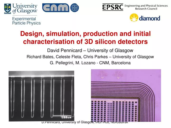
Design, simulation, production and initial characterisation of 3D silicon detectors. David Pennicard – University of Glasgow Richard Bates, Celeste Fleta, Chris Parkes – University of Glasgow G. Pellegrini, M. Lozano - CNM, Barcelona. 3D Detector Structure.

E N D
Design, simulation, production and initial characterisation of 3D silicon detectors David Pennicard – University of Glasgow Richard Bates,Celeste Fleta, Chris Parkes – University of Glasgow G. Pellegrini, M. Lozano - CNM, Barcelona D.Pennicard, University of Glasgow, INSTR08, Novosibirsk
D.Pennicard, University of Glasgow, INSTR08, Novosibirsk 3D Detector Structure • Array of electrode columns passing through substrate • Electrode spacing << wafer thickness (e.g. 30m:300m) • Benefits • Vdepletion (Electrode spacing)2 • Collection time Electrode spacing • Reduced charge sharing • More complicated fabrication - micromachining Planar 3D + + ve ve - - ve ve + + ve ve n n - - type type electrode electrode electrons electrons 300 300 300 300 µ µ m m µ µ m m holes holes p p - - type type electrode electrode Around Around Particle Particle µ µ m m 30 30
D.Pennicard, University of Glasgow, INSTR08, Novosibirsk Background • Invented in 1997 - S. Parker, C. Kenney, J. Segal • First produced in 1999 - Stanford Nanofabrication facility • Recent development: R&D towards experimental use • Improvements in micromachining make larger-scale, reliable production more feasible • Application: radiation-hard detectors for Super-LHC • 3D detector collaboration between Glasgow and CNM (Centro Nacional de Microelectronica, Spain) • Optimisation of 3D design through simulation • Fabrication of 3D detectors in CNM cleanroom • Initial characterisation • Overview of other 3D detector projects
D.Pennicard, University of Glasgow, INSTR08, Novosibirsk Super-LHC and Radiation Damage • RD50 collaboration – see G. Casse talk • Upgrade to LHC, planned for sometime after 2017 • 10x increase in luminosity • 10x increase in radiation damage • Inner layer of ATLAS pixel tracker will receive 1016neq/cm2 damage over SLHC running time Ian Dawson, University of Sheffield ATLAS upgrade workshop, Valencia, December 2007
D.Pennicard, University of Glasgow, INSTR08, Novosibirsk 3D Detectors and Radiation Hardness • Increase in effective p-type doping with damage • Increased depletion voltage • 300μm planar detectors cannot be fully depleted far beyond 1015neq/cm2 • 3D detectors have short depletion distance, reducing Vdep • Charge trapping • Free electrons and holes trapped by defects, reducing CCE • Dominant effect at very high fluences • 3D structure reduces collection time – less trapping • Increased leakage current • Need to cool detectors See M. Moll thesis, Hamburg 1999 G. Kramberger, Aug.23-24, 2006, Hamburg, Germany
D.Pennicard, University of Glasgow, INSTR08, Novosibirsk Simulation of 3D detectors after radiation damage • Simulations performed using Synopsys TCAD • Predict higher collection efficiency for 3D than for planar sensors • Model uses pessimistic values for trapping rates Plot compiled by M. Moll
D.Pennicard, University of Glasgow, INSTR08, Novosibirsk 3 column 8 column Optimisation of ATLAS 3D structure • ATLAS pixel is 400μm * 50μm • Different layouts available • Trade-offs between Vdep, CCE, capacitance, column area… Charge collection with 1016neq/cm2 radiation damage Capacitance at each pixel Bars show variation in CCE with hit position Smaller electrode spacing improves CCE
D.Pennicard, University of Glasgow, INSTR08, Novosibirsk Double-sided 3D detectors at CNM • Alternative 3D structure proposed by IMB-CNM • N- and p-type columns etched from opposite sides of substrate • Columns do not pass through full substrate thickness (in first production run) • 250μm deep in 300μm substrate • Recently finished production with p+ column readout and n-type substrate
D.Pennicard, University of Glasgow, INSTR08, Novosibirsk Double-sided 3D Detector production • Column fabrication introduces extra steps • Begin with columns on back side
D.Pennicard, University of Glasgow, INSTR08, Novosibirsk 250μm 10μm Double-sided 3D Detector production Hole etching • Deep Reactive Ion Etching • F plasma etches away base of hole • CF2 coating protects sidewall • Limit on depth : diameter ratio • 250m depth, 10m diameter
D.Pennicard, University of Glasgow, INSTR08, Novosibirsk (p+) n-Si Double-sided 3D Detector production Column filling and doping • Deposit 3μm poly-silicon • Phosphorus doping through poly • Passivate inside of column with SiO2
D.Pennicard, University of Glasgow, INSTR08, Novosibirsk Double-sided 3D Detector production Finished detector • P+ columns fabricated on front side • Contacts on front • Backside coated with metal for biasing 250μm 10μm
D.Pennicard, University of Glasgow, INSTR08, Novosibirsk Finished 3D devices Devices include: Pads, strips, pixels detectors, test structures Typical device layout – Strip detector, 80μm pitch 3D guard ring Bond pads Collecting electrodes Bias electrodes (back surface) 80μm
D.Pennicard, University of Glasgow, INSTR08, Novosibirsk Finished 3D devices SEM after polysilicon deposition and etching Pixel on Medipix detector Polysilicon and column (under passivation) Dry etching of the poly Polysilicon SiO 2 9.4mm Passivation (SiO2 and SiN) Bump-bond contact
D.Pennicard, University of Glasgow, INSTR08, Novosibirsk P+ N+ Lateral depletion around column (~2V in sim.) Initial tests - CV • Pad detector – 90 * 90 columns, 55μm pitch 2.3V lateral depletion Depletion to back surface from tip of column (~8V in sim.)
D.Pennicard, University of Glasgow, INSTR08, Novosibirsk P+ N+ Lateral depletion around column (~2V in sim.) Initial tests - CV • Pad detector – 90 * 90 columns, 55μm pitch 2.3V lateral depletion ~9V back surface depletion Depletion to back surface from tip of column (~8V in sim.)
D.Pennicard, University of Glasgow, INSTR08, Novosibirsk Initial tests – Strip detector IV • 128 strips, 50 holes/strip, pitch 80um, length 4mm • Measured with 3 strips and guard ring at 0V, and backside biased • Strip currents ~100pA (T=21˚C) in all 4 detectors • Can reliably bias detectors to 50V (20 times lateral depletion voltage) • Capacitance 5pF / strip • Guard ring currents vary: • Highest 20μA at 10V • Lowest 0.03μA at 50V
D.Pennicard, University of Glasgow, INSTR08, Novosibirsk Future work • Tests on these detectors • Charge collection test on strip detector with beta source and LHCb readout electronics • Tests before and after irradiation • X-ray detection test, using Medipix pixel readout (single-photon-counting) • New production run at CNM • Columns pass through full substrate thickness • Both p+ readout with n-substrate, and n+ readout with p-substrate • Includes ATLAS pixel detectors • Testbeams at CERN in summer • Collection performance vs position
D.Pennicard, University of Glasgow, INSTR08, Novosibirsk Other 3D detector projects • Stanford / Manchester / Sintef • FBK-IRST (Trento, Italy) • Glasgow / Diamond / IceMOS
D.Pennicard, University of Glasgow, INSTR08, Novosibirsk Stanford / Manchester / Sintef • First 3D detectors produced at Stanford Nanofabrication Facility • University of Manchester and CERN testing detectors • Have demonstrated good charge collection behaviour of ATLAS 3D pixels after SLHC radiation fluences • Working with Sintef (independent research foundation in Norway) to reproduce Stanford fabrication process on a larger scale Charge collection and signal/noise results Thanks to Cinzia da Via (Manchester)
D.Pennicard, University of Glasgow, INSTR08, Novosibirsk Stanford / Manchester / Sintef • “Active edge” electrode • Usually, silicon sensors have >100μm insensitive area at edge (need to avoid current flow from saw-cut edges) • Instead, plasma etch edge, and add a doped polysilicon layer • Edge acts as an electrode – dead area just 5μm • Achieve good coverage with fewer overlapping layers X-ray microbeam scan
Developments in Trento, Italy Double-side Double-Column 3D detectors Good results from preliminary electrical tests (C-V and I-V) First prototypes (p-on-n) completed, and n-on-p available soon.
D.Pennicard, University of Glasgow, INSTR08, Novosibirsk Glasgow / Diamond / IceMOS • Project between Glasgow and Diamond synchrotron to develop 3D detectors for X-ray crystallography • Single-photon-counting pixel sensors (Medipix, Pilatus) • Lower charge sharing in 3D detectors • Potential for thick 3D silicon detectors with good performance • Detectors produced in fabrication company IceMOS (Belfast) • First 3D detectors produced entirely in industry • Prototype run finished • Working test structures, but some problems with full devices • Starting second run with improved fabrication flow p-electrode (readout) n-electrode (bias)
D.Pennicard, University of Glasgow, INSTR08, Novosibirsk Conclusions • 3D detectors • Fast collection, low depletion voltage • Radiation hard – candidate for SLHC inner pixel layers • 3D production at CNM • First set of double-sided 3D detectors produced • Preliminary tests successful – continuing with charge collection tests • More production runs underway • Other 3D projects • Different groups working towards 3D detectors for high-luminosity colliders • Other applications possible, such as X-ray crystallography
D.Pennicard, University of Glasgow, INSTR08, Novosibirsk Thank you for listening
D.Pennicard, University of Glasgow, INSTR08, Novosibirsk First CNM 3D production run • P+ readout, n-type substrate devices on 4” wafer • 6 Medipix2 pixels Pitch 55μm, 256x256 • Single-photon counting sensor for medical X-ray detection (CERN) • 1 Pilatus pixel Pitch 172μm, 97x60 • Single-photon-counting sensor for X-ray crystallography (PSI) • 6 ATLAS pixels Pitch 50x400μm, 164x18 • Prototypes (wrong readout polarity) • 4 short strip Pitch 80μm, 50x50 • 1 long strip Pitch 80μm, 50x180 • Pad detectors, test structures
D.Pennicard, University of Glasgow, INSTR08, Novosibirsk Double-sided 3D detector – simulated behaviour • Where columns overlap, same behaviour as standard 3D • Weaker field near front and back surfaces – slower collection • Greater device thickness for given column length Electric field, 100V bias P+ N+
D.Pennicard, University of Glasgow, INSTR08, Novosibirsk Simulation of 3D detectors after radiation damage • Simulations performed using Synopsys TCAD • Predict higher collection efficiency than planar sensors • Model uses conservative values for trapping rates N-on-p results: PP Allport et al., IEEE Trans. Nucl. Sci., vol 52, Oct 2005
D.Pennicard, University of Glasgow, INSTR08, Novosibirsk Type Energy (eV) Trap σe (cm2) σh (cm2) η (cm-1) Acceptor Ec-0.42 VV 9.5*10-15 9.5*10-14 1.613 Acceptor Ec-0.46 VVV 5.0*10-15 5.0*10-14 0.9 Donor Ev+0.36 CiOi 3.23*10-13 3.23*10-14 0.9 Simulation methods • See presentation from 10th RD50 meeting • Synopsis TCAD finite element simulation • Damage model • Trap dynamics modelled directly • P-type FZ material • Based on work at Uni. Perugia – see M. Petasecca et al., IEEE Trans. Nucl. Sci., vol. 53, pp. 2971–2976, 2006 • Modified to match experimental trap times (V. Cindro et al., IEEE NSS, Nov 2006) Example of a simulated 3D structure n+ contact p+ contact oxide • βe= 4.0*10-7cm2s-1, βh= 4.4*10-7cm2s-1,
D.Pennicard, University of Glasgow, INSTR08, Novosibirsk N+ on p strip detector: CCE • At high fluence, simulated CCE is lower than experimental value • Trapping rates were extrapolated from measurements below 1015neq/cm2 • In reality, trapping rate at high fluence probably lower than predicted PP Allport et al., IEEE Trans. Nucl. Sci., vol 52, Oct 2005 900V bias, 280m thick From β values used, expect 25μm drift distance, 2ke- signal
D.Pennicard, University of Glasgow, INSTR08, Novosibirsk ATLAS 3D detector: CCE • Experiment used n+ readout, with 3 n+ columns per ATLAS pixel • Experiment used defocused IR laser pulse to flood the pixel with charge; the simulation mimics this • Both experiment and simulation show improved CCE at high fluence C. da Viaet al., Liverpool ATLAS 3D meeting, Nov. 06 Detectors produced at Stanford At high fluences, simulated CCE ~2/3 of experimental value (like with planar detector)
D.Pennicard, University of Glasgow, INSTR08, Novosibirsk Overview • Radiation damage model and comparison with experiment • Behaviour of different ATLAS pixel 3D layouts • Comparison of double-sided & standard 3D
D.Pennicard, University of Glasgow, INSTR08, Novosibirsk 3 50m 133m cell length 8 50m cell length ATLAS 3D simulations • ATLAS pixel (400m * 50m) allows layouts with different electrode spacing • No of n+ columns per pixel could vary from ~2-8 • Stanford have produced devices with 2-4 n+ columns • Previous ATLAS results shown used 3 columns • Simulations use 230m-thick p-type substrate, n+ readout • Columns have 5m radius, with dopant profile extending ~2m further • P-spray is used to isolate the columns 400m Spacing Note larger volume occupied by columns
D.Pennicard, University of Glasgow, INSTR08, Novosibirsk ATLAS 3D – Depletion voltage at 1016neq/cm2 • Depletion voltage will depend on substrate material (this model matches p-type FZ, rather than oxygenated silicon) • No. of n+ columns shown next to each data point • Vdep proportional to depletion distance squared
D.Pennicard, University of Glasgow, INSTR08, Novosibirsk ATLAS 3D – high-field voltage at 1016neq/cm2 • As an approximate judge of a “safe voltage”, found the bias at which the maximum field in each device reached 2.5*105V/cm • Surprisingly, all the devices gave much the same results at 1016neq/cm2 150V safe level
D.Pennicard, University of Glasgow, INSTR08, Novosibirsk Device structure and high-field regions • P-spray links p+ columns to n+ • So, the p-spray is at the same potential as the p+, resulting in high field at front surface where it meets the n+ columns • At higher bias the p-spray around the n+ column becomes depleted • These effects won’t be greatly affected by the electrode spacing itself 5-column ATLAS 3D, 1016neq/cm2, 150V bias 5-column ATLAS 3D, 1016neq/cm2, 150V bias Electrostatic potential (V) Doping conc. (cm-3)
D.Pennicard, University of Glasgow, INSTR08, Novosibirsk Device structure and high-field regions • P-spray links p+ columns to n+ • So, the p-spray is at the same potential as the p+, resulting in high field at front surface where it meets the n+ columns • At higher bias the p-spray around the n+ column becomes depleted • These effects won’t be greatly affected by the electrode spacing itself 5-column ATLAS 3D, 1016neq/cm2, 150V bias 5-column ATLAS 3D, 1016neq/cm2, 150V bias Doping conc. (cm-3) Hole conc. (cm-3)
D.Pennicard, University of Glasgow, INSTR08, Novosibirsk Charge collection vs position at 1016neq/cm2 • Simulated MIPs passing through detector at 25 positions, to roughly map the collection efficiency. Charge sharing not taken into account. 8 columns 6 columns
D.Pennicard, University of Glasgow, INSTR08, Novosibirsk Charge collection vs position at 1016neq/cm2 • Simulated MIPs passing through detector at 25 positions, to roughly map the collection efficiency. Charge sharing not taken into account. 4 columns 3 columns
D.Pennicard, University of Glasgow, INSTR08, Novosibirsk Average ATLAS CCE at 1016neq/cm2 • Average CCE found by flooding entire pixel with charge • Previous simulations used to find RMS variation from average, as a measure of nonuniformity. Shown by “error bars”. • CCE improves as electrode spacing is reduced (faster collection) Variation in collection with position larger relative to CCE
D.Pennicard, University of Glasgow, INSTR08, Novosibirsk Total capacitance seen at each ATLAS pixel • The total pixel capacitance was found with 1012cm-2 oxide charge (a typical saturated value) but without radiation damage. • C increases rapidly with no. of columns – the column capacitances add in parallel, and the capacitance per column gets larger as spacing decreases. Unlike in planar detectors, interpixel C is only a small component of total
D.Pennicard, University of Glasgow, INSTR08, Novosibirsk Signal to noise estimate at 1016neq/cm2 • Uses noise vs. capacitance data from unirradiated ATLAS sensors (won’t include high leakage current or damage to readout chip) • Assume 100fF from preamplifier input and bump bond • Also 70e- threshold dispersion Noise≈60e-+39e-/100fF Increasing C noise counteracts improving CCE “Progresses on the ATLAS pixel detector”, A. Andreazza, NIMA vol. 461, pp. 168-171, 2001
D.Pennicard, University of Glasgow, INSTR08, Novosibirsk Overview • Radiation damage model and comparison with experiment • Behaviour of different ATLAS pixel 3D layouts • Comparison of double-sided & standard 3D
D.Pennicard, University of Glasgow, INSTR08, Novosibirsk Comparison of double-sided & standard 3D • Full 3D (Parker et al., Stanford, Sintef, ICEMOS) • Double-sided 3D (CNM, Trento) • Readout columns etched from front surface • Bias columns etched from back surface • Columns don’t pass through full substrate thickness • The maximum column depth that can be etched is about 250m (with a 5m radius) • Double-sided 3D simulation uses 250m columns in a 300m substrate • Full-3D device used for comparison is 250m thick • Device structure used for comparison • N+ columns used for readout, p-type substrate • 55m* 55m pixel size (Medipix) • 100V bias n+ readout p+ bias
D.Pennicard, University of Glasgow, INSTR08, Novosibirsk Double-sided 3D field and depletion • Where the columns overlap, (from 50m to 250m depth) the field matches that in the full-3D detector • At front and back surfaces, fields are lower as shown below • Region at back is difficult to deplete at high fluence A. 1016neq/cm2, front surface 1016neq/cm2, back surface A. B. 100V 100V Undepleted B.
D.Pennicard, University of Glasgow, INSTR08, Novosibirsk Collection with double-sided 3D • Slightly higher collection at low damage • But at high fluence, results match standard 3D due to poorer collection from front and back surfaces. 20% greater substrate thickness
D.Pennicard, University of Glasgow, INSTR08, Novosibirsk High-field regions in full and double-sided 3D • Simulated full and double-sided 3D using p-spray isolation at 1016 neq/cm2 • Double-sided 3D is less prone to surface effects because columns are etched from opposite sides, but high-field regions develop at n+ column tip. Double-sided 3D Full 3D Field reaches 2.5*105V/cm at 170V Field reaches 2.5*105V/cm at 130V
D.Pennicard, University of Glasgow, INSTR08, Novosibirsk Type Energy (eV) Trap σe (cm2) σh (cm2) η (cm-1) Acceptor Ec-0.42 VV 9.5*10-15 9.5*10-14 1.613 Acceptor Ec-0.46 VVV 5.0*10-15 5.0*10-14 0.9 Donor Ev+0.36 CiOi 3.23*10-13 3.23*10-14 0.9 P-type FZ model – proton irradiation • See presentation from RD50 June 2007 • Based on work at Uni. Perugia – see M. Petasecca et al., IEEE Trans. Nucl. Sci., vol. 53, pp. 2971–2976, 2006 • Modified to give correct trapping times while maintaining depletion behaviour • Experimental trapping times for p-type silicon (V. Cindro et al., IEEE NSS, Nov 2006) up to 1015neq/cm2 • βe= 4.0*10-7cm2s-1 βh= 4.4*10-7cm2s-1 • Assume these can be extrapolated to 1016neq/cm2
D.Pennicard, University of Glasgow, INSTR08, Novosibirsk Comparison with experiment • Compared with experimental results with proton irradiation • Depletion voltage matches experiment • Leakage current is higher than experiment, but not excessive “Comparison of Radiation Hardness of P-in-N, N-in-N, and N-in-P Silicon Pad Detectors”, M. Lozano et al., IEEE Trans. Nucl. Sci., vol. 52, pp. 1468–1473, 2005 α=5.13*10-17A/cm α=3.75*10-17A/cm Experimentally, α=3.99*10-17A/cm3 after 80 mins anneal at 60˚C (M. Moll thesis)