Download
1 / 56
560 likes | 702 Views
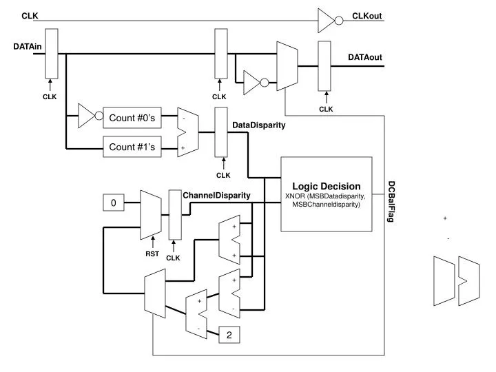
CLK. CLK. CLK. CLK. CLK. RST. CLK. CLKout. DATAin. DATAout. Count #0’s. -. DataDisparity. Count #1’s. +. Logic Decision XNOR (MSBDatadisparity, MSBChanneldisparity). ChannelDisparity. 0. DCBalFlag. +. +. -. +. +. +. -. -. 2. CLK. RST. CLK. CLK. CLKout. DATAin.

E N D
CLK CLK CLK CLK CLK RST CLK CLKout DATAin DATAout Count #0’s - DataDisparity Count #1’s + Logic Decision XNOR (MSBDatadisparity, MSBChanneldisparity) ChannelDisparity 0 DCBalFlag + + - + + + - - 2
CLK RST CLK CLK CLKout DATAin DATAout Count #1’s Bits (15:8) Data Disparity DataDisparity Count #1’s Bits (7:0) Logic Decision XNOR (MSBDatadisparity, MSBChanneldisparity) ChannelDisparity 0 DCBalFlag + + - + + + - + 2
Xn: 14 bits Xn_m: 14 bits Xn_m_k: 14 bits Xn_2m_k: 14 bits Clock 0 TrapzFilt Clock 3 25bits Sign MSearch RESETEvent Clock 4 Max
Trapezoidal Filter Xn: 14 bits Xn_m: 14 bits Xn_m_k: 14 bits Xn_2m_k: 14 bits Clock 0 + + + + Clock 1 + - Clock 2 + + Clock 3
<<1 Trapezoidal Filter and Pole zero correction Xn: 14 bits Xn_m: 14 bits Xn_m_k: 14 bits Xn_2m_k: 14 bits + + + + sum1 sum2 + - sub1 + + Result = si No pole zero correction New_prod(32:14) => New_prod / 16k + + Si(32) == ‘1’ Reset + + New_sum New_sum * 2 + New_result + New_sum * 3
AND <<1 Trapezoidal Filter and Pole zero correction ADC data: 14 bits Xn: 14 bits Xn_m: 14 bits Xn_m_k: 14 bits Xn_2m_k: 14 bits + + + + Energy clk clk sum1 sum2 LED + - clk New_prod(32:14) => New_prod / 16k sub1 + + + + clk clk Threshold Result = si No pole zero correction New_result + + AboveTh PZEnable clk LED Reset AboveTh LED Reset New_sum Double Correlation Enable New_sum * 2 + + - + New_sum * 3 clk To Energy max/min search
Trapezoidal Filter and Prog.Pole zero correction ADC data: 14 bits Xn: 14 bits Xn_m: 14 bits Xn_m_k: 14 bits Xn_2m_k: 14 bits + + + + LED clk clk sum1 sum2 LED + - clk New_prod(32:14) => New_prod / 16k sub1 + + + + clk clk Threshold Result = si No pole zero correction New_result + + AboveTh clk PZEnable Reset New_sum To Energy max/min search Prog PZ multiplier x x - clk
Xn: 15 bits Pipe 1 Xn-1: 15 bits Pipe 2 Xn-2: 15 bits + 1 0 Sum: 16 bits + Pipe 3 + Pipe 4 Yn: 17 bits
Main FPGA requirements FIFO DAC Channels ADC FIFO Interface DAC Control VME Control VME FPGA ADC ADC ADC Front Bus Logic ADC FB Buffer ADC ADC C.C. PileUp Master Logic ADC C.C. LED SD Chip EN ADC Master LogicEnable ADC
Main FPGA LEDs Aux. IO FIFO DAC CH. 9 ADC FIFO Interface DAC Control VME Control VME FPGA CH. 8 ADC CH. 7 ADC CH. 6 ADC Front Bus Logic CH. 5 ADC CH. 4 ADC FB Buffer CH. 3 ADC C.C. PileUpm CC_LED, CC_energy_ready Master Logic CH. 2 ADC CC_TS, CC_Energy SD Chip EN CH. 1 ADC Master LogicEnable CH. 0 ADC
Debug Data Validate ADC Data LED TapDelay1 TapDelay2 Energy CFD TapDelay3 circular buffer 40us 7 BRAM ENERGY CFD Data TapDelay4 Circular Buffer ProcCore Header Memory Pre-Buffer 8BRAM * 10 ch = 80 1Multiplier * 10ch = 10 Total is 90 out of 96.
. . . HMWrSel EnHM HMRdSel DataSel PileUpCounter EN Header Memory1 Trigger/Validate PREBUFFERDATA LEDTimeStamp Timing SM Header SM Package SM TimeOutFlag EN Header Memory16 Size CBStartAddr WaitCounter PreBufferAdderss CFD_TS CFDTimeStamp LED_TS Timer FBLED_TS FB_LED TimeOutFlag Board_ID Energy CFD1 CFD2 CircBufferAddress Raw Data CircularBuffer
Header Memory (HM) Diagram Header Data FIFO Read_EN Write_EN Pre Buffer Data_out Header Memory SM Validate Channel SM Status ExternalValidation Timer StartExternal ValidationWait
Timing State Machine TapDelayValid & Enable = 1 & LED or Validate ProgramFlag Program IDLE Trigger ProgramACK WaitCounter
Header Memory State Machine BoardId ComputeDone & NoPileUP Size LED_TS IDLE LED_TS LED_TS ENERGY Prebuffer StartPosition CFD_TS CFD_TS SlidingDone CFD_TS Sliding CFD1 WaitCounter CFD1 CFD2 CFD2
Package State Machine PreBufferReady & ExternalValidation & Validate HMValid BoardId Size IDLE LED_TS LED_TS LED_TS RawData ENERGY CFD_TS CFD_TS CFD_TS LoadCB StarAddress CFD1 CFD1 Sliding CFD2 CFD2
FIFO Interface Stay until done Stay until done Channel 0 Channel 1 Stay until done Stay until done Channel 9 Channel 2 Start/done Start/done Start/done Start/done Stay until done Stay until done Channel 8 Channel 3 Start/done Start/done 9 Bit Counter Start/done Start/done Start/done Start/done Channel 4 Channel 7 Stay until done Stay until done Channel 5 Channel 6 Stay until done Stay until done
Front Bus Logic Diagram (slave) VME Control Other_Status(9:0) Slave Registers Time Stamp(47:0) FB_Data(9:0) FB_Address(7:0) LED_Status(9:0) FB_Strobe* FB_RNW Master FB FB_Data_Dir FB_Data_EN Clear Hit Pattern Channels Front Bus SM FB_LED SLAVE_Board_ID HM_Validate, FB_Sync HM_Address(3:0) Slave Header data package TS_FB_LED Slave Header Data When the Master Logic is disabled the signals are Just routed to the outside buffers.
Front Bus State Machine Diagram (slave) ReceivedValidCmd (FB_cmd = Valid & FB_add = 000 or MyAdd) ReceivedValidCmd (FB_cmd = Valid & FB_add = 000 or MyAdd) READ IDLE SET DATA 100MHz WAIT WAIT Master Write Master Read IDLE Comp TS Set Flag 50MHz SetCal ChargeInject LatchStatus
Front Bus Timing Diagram WRITE READ FB_CLK FB_ADD FB_RNW FB_ACTIVE* FB_DATA Master Data Slave Data
CLK CLK Address XX Address XX Address XX Address XX XX XX XX XX RNW RNW Strobe* Strobe* DATA ZZ DATA ZZ Data ZZ Data ZZ Write Operation Read Operation
VME Diagram ProgFlag ReadRegFlag Latch VME Signals ProgFlag ReadRegFlag ProgFlag ReadRegFlag ProgFlag ReadRegFlag Channels VME FPGA ProgFlag ReadRegFlag ProgFlag ReadRegFlag ProgFlag ReadRegFlag FIFO CLK50 ProgFlag ReadRegFlag VME SM ProgFlag ReadRegFlag ProgFlag ReadRegFlag
DAQ Diagram Front Bus SM VME Interface DAC Chips CH0 Channels DATA CH9 Constant value
DAQ State Machines ProgFlag = ‘0’ IDLE Prog RegFlag = ‘0’ IDLE Verify Addr RegAddr = MyAddr DataReceived = ‘1’ Write Data
Master Logic Diagram SD Chip Fast Data CH0 CC LED & PileUp CC LED & PileUP Flags Master Logic Registers SD Tx Logic SD Chip ch’s TTCL Main Logic Master Logic Header Front Bus SD Rx Logic FB Slave Data Status FB Driver Ctrl. Sig. MasteSlave Logic VME Control
Serdes Logic Diagram CC PileUp Fast Data CH9 CC LED SD Tx Logic SD Chip TTCL Main Logic SD Rx Logic Data Status Ctrl. Sig.
Master Front Bus Diagram FB_Data(9:0) FB_Address(1:0) FB_cmd(3:0) Master Main Logic FB_Data_Dir Front Bus High Level Logic Front Bus Low Level SM FB Buffer Enabled FB_Data_EN Command Command_FLag Command_ACK FB_CTRL_Dir Busy Enabled FB_CTRL_EN Data_Out Data_IN FB_Data(9:0) FB_Address(1:0) NewCmd Address RNW FB_cmd(3:0) Busy FB_Data_Dir RegAddress1 Slave FB Registers FB_Data_EN RegData ProgFlag ProgAddr FB_CTRL_Dir ProgData FB_CTRL_EN ProgAck Reg0 . . . RegData RegN RegAddress1
Front Bus State Machine Diagram (master) Write TS 0 DISABLED Write TS 1 IDLE Write TS 1b FBLL_Busy Write TS 2 SetGet Slow Data 0 Wait FBLL_Busy Write TS 3 Get Slow Data 0 FBLL_Busy FBLL_Busy Cmd Register Write TS 4 SetGet Slow Data 1 FBLL_Busy Clear HitPattern Write TS 5 Get Slow Data 1 FBLL_Busy Write TS 6 SetGet Slow Data 2 FBLL_Busy Write TS 7 Get Slow Data 2 Wait Save Data FBLL_Busy Write TS 8 SetGet Slow Data 3 Write Debug Data Wait data FBLL_Busy Write TS 9 Get Slow Data 3 Read Debug Data FBLL_Busy Write TS 10 Save Last hitpattern 100MHz
Front Bus Low Level State Machine Diagram (master) DISABLED NewCmdFlag & RNW* NewCmdFlag & RNW SET CTRL IDLE SET CTRL SET DATA WAIT1 WAIT Latch Data WAIT2 50MHz
FB_SM Low Level Flags SendCmd CLK RST Done ARST SET ARST BusyFlag NewCmdAck NewCmd CLK RST ARST SET ARST NewCommandFlag
Master Logic Front Bus State Machine Stay until Done IDLE Send Command Receive Board 0 Stay until Done or Timeout Receive Board 3 Send Command Stay until Done or Timeout Stay until Done or Timeout Send Command Receive Board 1 Stay until Done or Timeout Stay until Done or Timeout Receive Board 2 Send Command Stay until Done or Timeout Stay until Done or Timeout
SD Rx Diagram RX State Machine Command_Ready (‘1’ if cmd != Null) SD_RPDWN Package_error SE_Lock SD_EN SD_Lock DemuxAddress Data DataRdy Master Main Logic FIFO DCBal Logic Cor. Command Rebuilder (demux) SD_RX_CLK50 SD Chip DATA 5x16 SD_RX_Data_IN BRAM
SD Rx State Machine Reset NewCmdReady Disabled SD_EN & SD_Lock_N* Wait Sync Debug Package Error End-of-cicle Trigger Spare Trigger Spare Trigger Auxiliary Trigger SD_EN & SD_Lock_N* Reset Spare Trigger ReadSyncCmd WaitSyncCmd Disabled Async Trigger Internal Trigger Word 1 Slow Data Trigger Word 2 Internal ReSyncCmd Spare Word 3 NewCmdReady Word 4 Word 0
SD_RX_SM Flags ReadSyncCmd PackageError CLK RST ARST SET ARST ReSyncCmd
SD Rx Snap Shot Memory RST CLK Bram CLK50 ReadEN SD Chip SD Main Logic Data Data Busy Empty StartRec Address In Address out Busy
SD_RX_ Snap Shot Memory Flags StartRecording AddressIn CLK RST ARST SET ARST Busy AddressOut CLK RST Busy SET SET ARST Empty
SD Tx Diagram RST CLK CLK50_IN Reset Buffer Cnt TX State Machine Package Latched SD_Lock_N Counter_EN / Counter rest Package_Ready SD_Sync SD_EN SD_TPDWN_N DemuxAddress GrayCounter DataFlag XTAL_ID DC Bal. Add Fast Data BufferCnt SD Main Logic CLK50 SD Chip DCBalWord Data Data Pack. DATA 13x8 Error CC LED Fast Data CH9 CC PileUp
SD Tx State Machine Reset DataPack_TX_EN* Disabled DataPack_TX_EN XTAL_ID. Buffer_Count DC Bal. word Spare DataPack_TX_EN* DC Bal. word Hit Pattern A DC Bal. word Hit Pattern B SD_EN Reset DC Bal. word Hit Pattern C PackageReady& HasPackage* IDLE DC Bal. word Hit Pattern D DC Bal. word Hit Pattern E LatchData Lock_N DC Bal. word/Spare TS (Low byte) DC Bal. word/Spare TS (High byte) SYNC ResetBuffer Cnt CCEnergy (HB) CCEnergy (LB)
SD_TX_SM Flags PackageReady PackageSent CLK CLK RST RST P P ARST SET ARST ARST SET ARST HasPackage LatchDataSig CLK RST P P SD_EN DataPack_TX_EN ARST SET ARST ResetBufferCntsig Lock_N
Main Logic Diagram VME Interface Cmd FB Control Data DataReady SD TX Main State Machine TS Data Counter_EN TS Memory Counter Counter_RST Readout_cmd Command ready Comparator Data Pack. Comp_EN SD RX TTCL TS Counter Readout_cmd TS WR_EN FIFO TS Trigger Decision Status TS State Machine FIFO_Empty SystemInSyncFlag Comp. RD_EN CC TS
Main Logic Diagram FB Control Cmd VME Interface Data_TX Data_Rx DataReady SD TX Fast Flags & Status byte Latch Energy and TS_LB and TS_HB TS Memory Block CC_LED Processing Core SD RX Readout_cmd TS Data Command ready EnergyReady HM Position TS & CompType Latch CC TS TTCL TS CompType TS WR_EN Load TS Sync Comp FIFO TS Trigger Decision FIFO_Empty SystemInSyncFlag CC_LED TS Data RD_EN CC TS
Time stamp memory Block Diagram TS, HMPos, Load T155, T15A, T1A5, T255,T25A,T2A5 TS Memory Registers Main State Machine Comparator (48bits) TS CompType HM_Pos StartComp ReadoutCmd Erase Count Counter (4 bits) CompDone CompResult CompType+TS AckReadoutCmd WR_EN FIFO_DataOut FIFO TS Trigger Decision Add1 TS State Machine FIFO_Empty ClearCounter RD_EN Status Empty #ofMem occupied
Time stamp State Machine Count = “1111” Add 1 Reset FifoEmpty* and TSMemoryEmpty* Count != “1111” CompResul* StartComp IDLE Compare CompDone* FifoEmpty* and TSMemoryEmpty StartComp CompResul Remove FIFO Data Readout cmd Ack*
Time stamp memory Registers Diagram TS_Datain Empty_0 TS_MemoryEmpty Empty_1 LD_0 Empty_15 Load Load Logic TS Mem. Cell 0 LD_1 HM_Pos_LD HM_Empty TS Mem. Cell 1 LD_15 . . . TS_Dataout ER_0 Erase Logic ER_1 Erase ER_15 TS Mem. Cell 15 HM_Pos_Rd
Time stamp memory Cell Diagram Load Register TS_Datain TS_Dataout Erase TimeoutFlag TS_MemoryEmpty EmptyFlag EmptyFlag Timer TimeoutFlag EmptyFlag
CLK CLK CLK CLK CLK Time stamp memory Comparator (48 bits) TS_FIFO TS_Datain TS_FIFO + Comp B ≥ A B A T155 T15A + T1A5 CompType TS_MemoryEmpty + Comp B ≥ A A B T255 T25A - SM CompDone T2A5 StartComp
Time stamp memory Comparator (48 bits) TS_FIFO TS_Datain TS_FIFO + Comp B ≥ A B A T155 T15A + T1A5 CompType TS_MemoryEmpty + Comp B ≥ A A B T255 T25A - CompDone Vcc T2A5 StartComp
Time stamp memory Comparator (48 bits) Reset StartComp* StartComp Comp 1 IDLE StartComp Comp 2 StartComp* Comp 3 CompDone
Processing Core VME Interface SD TX Registers Registers Registers SD RX Registers TS Memory Block State Machine FB Control FIFO TS Trigger Decision CC TS