Download
1 / 24
260 likes | 502 Views
Series Resonant Converter with Series-Parallel Transformers for High Input Voltage Applications. C-H Chien 1 ,B-R Lin 2 ,and Y-H Wang 1 1 Institute of Microelectronics, Department of Electrical Engineering, National Cheng-Kung University, Tainan 701, Taiwan

E N D
Series Resonant Converter with Series-Parallel Transformers for High Input Voltage Applications C-H Chien1,B-R Lin2,and Y-H Wang1 1 Institute of Microelectronics, Department of Electrical Engineering, National Cheng-Kung University, Tainan 701, Taiwan 2 Department of Electrical Engineering, National Yunlin University of Science and Technology, Yunlin 640, Taiwan
Outline • Introduction • Circuit configuration • Experimental results • Conclusion
What’s for in this study? • For 3-phase 380V (or 480V) AC/DC converters • the DC bus voltage > 500V (or 650V) • ∴ select suitable power MOSFETs → difficult • 3 level neutral-point clamp converter →overcome these drawbacks • more power switches • more circuit components • high cost • complicated control schemes • split capacitors and clamp diodes • the Vstress of MOSFETs → ½ DC bus voltage
What’s new in this study? • A novel DC/DC converter (24V/40A, 960W) • 2 circuit modules for high voltage application • 2 capacitors and 2 half-bridge • series in high Voltage • clamp the Vstress of MOSFET • Vstress = ½ input V • interleaved switching signal → phase-shift ¼ switching T → 90° • reduce ripple current (input and output) • share the load current • reduce the size of magnetic core
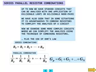
Why is the topology ? • A series resonant tank • high conversion efficiency • high power density • 2 series Transformers • balance the 2 winding current • all semiconductors soft switching • switching loss ↓ • ∵ (ZVS & ZCS) • wide input voltage and load • 480V~600V • all load • 2 windings in parallel • Istress ↓
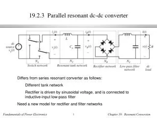
Circuit configuration and key waveforms • Circuit configuration • Key waveforms
Different modes during 1 period • Mode 3 • Mode 5 • Mode 1 • Mode 2 • Mode 4 • Mode 6
Mode 1 ( t0≦t<t1 ) • S1 off , S2 → off • VLm1=nVo= VLm2 • Cs1, Cs2, and Lr1 → resonant • iLr1 • Cs2=> from 0 V → Vin/2 → charge • Cs1=> from Vin/2 → 0 V → discharge • iLm1 → • iLm2 → • iD1 → • iD3 →
Mode 2 ( t1≦t<t2 ) • S2 off , S1 → ZVS→ on • iLm1= iLm2= iLr1 →mode end • VLm1=nVo= VLm2 • Cr1 and Lr1→ resonant • applied voltage = (Vin/2-2nV0) • iLm1 ,iLm2 • linearly ↑ • slope = nV0/Lm • iLr1 → • Vcr1→
Mode 3 ( t2≦t<t3 ) • S2 off , S1 → on → off • iLm1= iLm2= iLr1 →mode start • S1 off →mode end • iD1=iD2=iD3=iD4=0 • Cr1, Lr1, Lm1, and Lm2 → resonant • iLr1 → • Vcr1 →
Mode 4 ( t3≦t<t4 ) • S2 off , S1 → off • VLm1=-nVo= VLm2 • Cs1, Cs2, and Lr1 → resonant • iLr1 • Cs1 => from 0 V → Vin/2 → charge • Cs2 => from Vin/2 → 0 V → discharge • iLm1 ,iLm2 • linearly ↓ • slope = -nV0/Lm • Vcs1 → • Vcs2→ • iD2 → • iD4 →
Mode 5 ( t4≦t<t5 ) • S1 off , S2 → ZVS → on • iLm1= iLm2= iLr1 →mode end • VLm1=-nVo= VLm2 • Cr1 and Lr1→ resonant • applied voltage = 2nV0 • iLm1 ,iLm2 • linearly ↓ • slope = -nV0/Lm • iLr1 → • Vcr1→
Mode 6 ( t5≦t<t0 ) • S1 off , S2 → on → off • iLm1= iLm2= iLr1 →mode start • S2 off →mode end • iD1=iD2=iD3=iD4=0 • Cr1, Lr1, Lm1, and Lm2 → resonant • iLr1 → • Vcr1 →
Key circuit parameters of the prototype circuit • Input voltage Vin → 480V ~ 600V • Input nominal Vin,norm → 530V • Output voltage Vo and current Io → 24V / 40A • Series resonant frequency fr → 100kHz • Switches S1~S4 → IRFP460 • Diodes D1~D8 → MBR3060PT • Turns ratio of T1~T4 → np:ns1:ns2=20:6:6 • Resonant inductances Lr1~ Lr2 → 21 μH • Magnetizing inductances Lm1~ Lm4 → 82 μH • Resonant capacitances Cin1~ Cin2 → 330 μF/400V • Output capacitances Co → 2200 μF/50V
The interleaved signals of switches • Experimental waveforms of gate voltages • S1~S4at full load • Vin=530V
The ZVS of switches under input 530V • Experimental gate V, drain V and drain I of switch S1 • Vin→ 530V • load → 25% • Experimental gate V, drain V and drain I of switch S1 • Vin→ 530V • load → 100%
The ZCS of rectifier diodes under input 530V • Measured waveforms of gate voltages • vS1,gsand vS3,gs • Output currents of each center tapped rectifier • at full load • nominal input voltage • Vin=530V • turn off • ZCS
Switching Frequency VS. Output Power • Measured switching frequencies • at different input voltages • at different load
The voltage stress of each switch=0.5Vin balance 2 winding current share the load current switching loss↓ Conclusion • A resonant converter • with the series half-bridge legs • for high DC bus voltage application • Two circuit modules • share the load power • For each module • series-connected in primary side • parallel-connected in secondary side • power MOSFETs → turn on ZVS • rectifier diodes → turn off ZCS