Download
1 / 41
520 likes | 2.42k Views
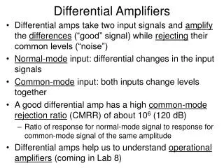
Differential Amplifiers and common mode feedback. Differential amplifiers. Cancellation of common mode signals including clock feed-through Cancellation of even-order harmonics Increased signal swing Symbol:. Two-Stage, Miller, Differential-In, Differential-Out Op Amp. peak-to-peak

E N D
Differential amplifiers • Cancellation of common mode signals including clock feed-through • Cancellation of even-order harmonics • Increased signal swing Symbol:
Two-Stage, Miller, Differential-In, Differential-Out Op Amp peak-to-peak output voltage ≤ 2·OCMR Output common mode range (OCMR) = VDD-VSS - VSDPsat - VDSNsat
Two-Stage, Miller, Differential-In, Differential-Out Op Amp with Push-Pull Output Able to actively source and sink output current Output quiescent current poorly defined
Differential-Output, Folded-Cascode OCMR = VDD -VSS - 2VSDP(sat) -2VDSN(sat) Quite limited
Two-Stage, Differential Output, Folded-Cascode M11-M13 and M10-M12 provide level shift
Common Mode Output Voltage Stabilization Common mode drift at output causes differential signals move into triode region
Common Mode feedback • All fully differential amplifier needs CMFB • Common mode output, if uncontrolled, moves to either high or low end, causing triode operation • Ways of common mode stabilization: • external CMFB • internal CMFB
Cause of common mode problem Unmatched quiescent currents Vbb=VbbQ+Δ Vbb I2 Vin=VinQ Vbb=VbbQ Vo1 Vo2 Vin I1 Vo1Q Vo1 Vin=VinQ+ΔVin actual Q point M2 is in triode
Vxx Ix Vo Ix(Vo) VOCM Vin Iy(Vo) Vyy Iy Vo
Basic concept of CMFB: CM measurement Vo+ +Vo- 2 Vo+ Vo- Voc - CMFB Dvb e VoCM + desired common mode voltage
Basic concept of CMFB: CM measurement Vo+ +Vo- 2 Vo+ Vo- Voc - CMFB Dvb e e VoCM + Find transfer function from e to Voc, ACMF(s) Find transfer function from an error source to Voc Aerr(s) Voc error due to error source: err*Aerr(0)/ACMF(0)
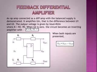
example Vb2 CC CC Vi+ Vi- Vo+ Vo- VCMFB Vb1 Vo+ VCMFB Voc - Vo- +
Example Voc ? ? VoCM Need to make sure to have negative feedback
VDD M7A 150/3 150/3 M2A M2B 300/3 300/3 75/3 M13A M13B BIAS4 averager 1.5pF 1.5pF M7B 75/3 M3B BIAS3 OUT+ OUT- 20K 20K M3A 300/2.25 300/2.25 300/2.25 300/2.25 M6C 75/2.25 IN- IN+ Source follower M1A M1B M12B M6AB M12A 1000/2.25 75/2.25 1000/2.25 200/2.25 BIAS2 M11 M10 M9A M9B CL=4pF 4pF 150/2.25 50/2.25 50/2.25 BIAS1 M8 M5 200/2.25 M4A M4B 150/2.25 50/2.25 50/2.25 VSS Folded cascode amplifier
Resistive C.M. detectors: R1 R2 Vo+ Vo-
Resistive C.M. detectors: Vo.c. R1 R1 Vo+ Vo- Vi+ Vi-
O.K. if op amp is used in a resistive feedback configuration • & R1 is part of feedback network. • Otherwise, R1 becomes part of g0 & hence reduces AD.C.(v)
Buffer Vo+, Vo- before connecting to R1. Voc Vo+ Vo- R1 R1 Simple implementation: source follower Vo.c. Vo+ Vo- * Gate capacitance is your load to Amp.
Why not: Vo.c. Vo+ Vo- * Initial voltage on cap.
C1 C2
Use buffer to isolate Vo node: gate cap is load or resistors
Switched cap CMFB Vo+ Φ1 Φ2 Φ1 VoCM. Vo- VoCM.
To increase or decrease the C.M. loop gain: e.g. Vo.c. Vo.c.d. Vo.c. Vo.c.d. VC.M.F.B. VC.M.F.B.
Another implementation • Use triode transistors to provide isolation & z(s) simultaneously. M1, M2 in deep triode. VGS1, VGS2>>VT Voc Vo+ Vo- M1 M2 In that case, circuit above M1, M2 needs to ensure that M1, M2 are in triode. can be a c.s.
Example: Input state Vo+ Vo- Vb M1 M2 e.g. Vo+, Vo-≈2V at Q & Vb≈1V , Then M1&2 will be in deep triode.
Vo- Vo+ Vb1 Vb2 VX M1 M2
Two-Stage, Miller, Differential-In, Differential-Out Op Amp M10 and M11 are in deep triode
Vo++ Vo- 2 VoCM. VCMFB Vo+ Note the difference from the book accommodates much larger VoCM range Vo-
Small signal analysis of CMFB Example: IB IB VCM M4 M3 Vo+ Vo- M1 M2 -Δi +Δi +Δi +Δi M5 +Δi -Δi -Δi -Δi VCMFB Δi=0 2Δi
Differential Vo: Vo+↓ by ΔVo, Vo-↑ by ΔVo • Common mode Vo: Vo+↑ by ΔVo, Vo-↑ by ΔVo
IB IB VCM M4 M3 Vo+ Vo- M1 M2 +Δi +Δi M5 -Δi -Δi VCMFB Δi=0 2Δi M7 Δi7 + - 1 gm6 -2Δi -2Δi M6
CMFB loop gain: example Vb2 CC CC Vi+ Vi- Vo+ Vo- VCMFB Vb1 Vo+ VCMFB Voc - Vo- +
-gm5vro2 -gm5vro2gm6 Vo gm5v v Poles: p1 p2 z1 same as before
VDD M7A 150/3 150/3 M2A M2B 300/3 300/3 75/3 M13A M13B BIAS4 averager 1.5pF 1.5pF M7B 75/3 M3B BIAS3 OUT+ OUT- 20K 20K M3A 300/2.25 300/2.25 300/2.25 300/2.25 M6C 75/2.25 IN- IN+ Source follower M1A M1B M12B M6AB M12A 1000/2.25 75/2.25 1000/2.25 200/2.25 BIAS2 M11 M10 M9A M9B CL=4pF 4pF 150/2.25 50/2.25 50/2.25 BIAS1 M8 M5 200/2.25 M4A M4B 150/2.25 50/2.25 50/2.25 VSS Folded cascode amplifier
Removing the CM measurement Vo+ VoCM Vo- VCMFB Directly connect Vo+, Vo- to the gates of CMFB diff amp.
VDD=+1.65V M11 M12 M3 M4 M26 M27 Vo1 Vo2 M21 M22 M23 M24 M1C M2C IDC=100υA VCM M13 Vi1 M2 Vi2 M1 M14 M51 M52 M25 -VSS=-1.65V
CMFB with current feedback M3 M4 IB Vo+ Voc CM detect VoCM Vo- M5 M6 M7 M1 M2