Download
1 / 15
180 likes | 535 Views
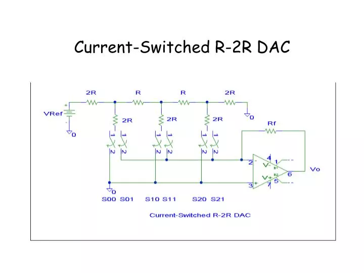
Current-Switched R-2R DAC. Voltage-Switched R-2R DAC. DAC Non-Linearities. DAC Gain & Offset Errors. Direct (Flash) ADC. n-bit conversion in n clock cycles (n+1) bit conversion if comparator output used. Comparator. Analogue Input. Logic. Digital Output. DAC. 100(1). 110(0). 101(1).

E N D
n-bit conversion in n clock cycles (n+1) bit conversion if comparator output used Comparator Analogue Input Logic Digital Output DAC 100(1) 110(0) 101(1) Clock Successive Approximation ADC Successive Approximation ADC
Integrating ADCs • ·There is a whole family of these circuits: • osingle-slope • odual-slope • omulti-slope • ocharge balance, PWM • osigma-delta (-) (order 1 to m) • None need a T(S)/H, (but may be useful) • All integrate the input signal for a fixed time and then digitize it • [conversion time up to 2 x 2n = 2n+1 clock periods] • However, the last 2 types integrate continuously • All allow increased resolution but are slower than the - type
VC 2n clock periods (2nT) m clock periods (mT) Time V -VREFt/R -VINt/R V = (2nT)VIN/R = mTVREF/R VIN/VREF = m/2n (n-bit conversion) Dual-Slope Multi-Slope Integrator Output Voltage Waveforms Integrator Output Waveforms
Multi-Slope ADC • To increase resolution, the comparator threshold becomes the limiting factor • Multi-slope uses smaller and smaller reference values to progressively approach the comparator zero at a slower rate • Each reference period ‘de-integrates’ the remaining error • Very much more complex circuit and costly • Much faster than Dual-Slope for the same resolution - used in some DVMs • May also be used with Charge-Balance
T mT Clock -(VIN/R)t/C -[(VIN/R) + I0]t/C Integrator Output V Comparator Output D-Type (Q) Output Integrator Output Waveforms
Charge Balance Performance • Integrates signal and ‘reference’ signals continuously • I0 = VREF/R then VIN = VREF.Count/CountMax • Reduces integrator capacitor error of Dual-Slope • Capable of 10-8 (26-bit) performance, if you can wait - speed v resolution • DVM type ADC [PWM variants]
Sigma-Delta ADC (1) • Recent variant of Delta modulator and Charge-Balance concepts • Originally used for audio only, now used from dc to rf • Very high resolution up to 22bits and very fast … 1000x faster than dual-slope • Very complex internal operation but quite simple analog circuitry • Uses a special (decimating) digital filter • Can be integrated with µCs etc • Minimal chip cost but support circuits still expensive for ultra-high performance
Functional Diagram of 3rd order Sigma-Delta ADC LTC2440 Sigma-Delta ADC (2)