Solid State Physics
670 likes | 2.09k Views
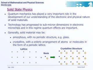
Crystalline Structure. Lattice. Basis. +. Solid State Physics. Quantum mechanics has played a very important role in the development of our understanding of the electronic and physical nature of solid materials.

Solid State Physics
E N D
Presentation Transcript
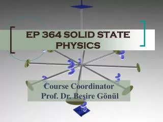
Crystalline Structure Lattice Basis + Solid State Physics • Quantum mechanics has played a very important role in the development of our understanding of the electronic and physical nature of solid materials. • Technology has progressed to sub-micron dimensions in electronic microchips and in this regime quantum effects are important. • Generally, solid material may be: • amorphous, with no periodic structure, e.g. glass. • crystalline, with a orderly arrangement of atoms or molecules in the form of a periodic lattice.
Crystals • Crystalline materials are theoretically tractable due to the presence of long range order in the lattices. • There are 14 different standard crystal lattices, three of which are shown below. Face centred cubic lattice. Simple cubic lattice. Body centred cubic lattice.
Example - NaCl Crystal • Face centred cubic structure that repeats. • Similar sharing of electrons as in molecular bonding. Each Na+ ion is surrounded by 6 Cl- ions and vice versa. • Potential function has both attractive and repulsive components (as for molecules): • a is known as the Madelung constant and has a value of 1.75 for NaCl; m is a small integer. • NaCl has an equilibrium distance ro between ions at which the ionic cohesive energy (energy/ion to disassemble solid into separate ions) is:
Metalic Solids • The bulk of the elements are metallic in nature. • In general metallic elements form crystalline structures which are relatively close-packed such as hexagonal close packing, body centred cubic, or face centred cubic • The outermost electrons of metallic atoms are weakly bound. When these atoms come together to form crystalline structures, the loosely bound electrons are relatively free to move among the atoms as an electron ‘gas’. • Since the atoms ‘lose’ their outermost electrons, they are essentially positive ions.
Metallic Solids (ctd) • According to current metallic bond theory the metalic structure is held together by the electrostatic attraction between the positive ions and the negatively charged electron ‘gas’. • The electron ‘gas’ is also thought to be responsible for the high electrical and thermal conductivities, surface luster and other metallic properties. • Since the outermost electrons are free to move among the ions, they do not belong to any single atomic bond. It is therefore possible to alloy different metals provided their atoms are similar in size.
Free electron theory of metals • Electrons that are free to move in a piece of metal may have an extremely large number of energy states available to them. • It is as if the electrons are trapped in a finite well whose width L is of the size of the piece of metal and, therefore, very large compared to atomic dimensions. • The electron energy is therefore quantised (as in the case of a one dimensional finite well) and, since L is very large, the allowed energy levels are very closely spaced. • The “density of states” g(E) provides a statistical means of dealing with the large number of states which are available. • g(E)represents the number of states per unit volume per unit energy interval. For infinite square well:
3 p 8 2 m 2 1 = g ( E ) E 2 3 h Free electron theory of metals (ctd) • g(E)dE represents the number of states per unit volume that have energy between E and E + dE • The density of states g(E) is given by • For a 1cm cube of Copper, the number of states in the range 5.0-5.5eV is:
Occupancy of States - Fermi-Dirac statistics • In keeping with the exclusion principle, two electrons cannot be in the same state if they have the same set of quantum numbers. • A given state can therefore accommode only two electrons, one with spin +1/2 and the other with spin -1/2. • A consequence is that, at zero Kelvin, the energy states are filled from the zero energy level, with two electrons per state, until all electrons are accounted for. The last occupied state is called the Fermi level and the corresponding energy is called the fermy energy EF.
Occupancy of States - Fermi-Dirac statistics (ctd) • EF is determined by integrating the density of state expression for energy over the interval from E =0 up to E= EF. • N/Vis the number of conduction electrons per unit volume in the metal • Copper has EF = 7.0eV and Eaverage = 4.2eV. Energy from thermal motion is 3/2kT=0.04 eV. • As the temperature increases, it is expected that the electrons will gain thermal energy and occupy energy states above the Fermi level. The probability of an energy state E being occupied is given by the Fermi factor f(E)
1 E < Ef • At T = 0 K, f(E) = 0 E > Ef Fermi-Dirac Probability Function i.e. all states are occupied up to the Fermi level (probability f(E) =1) • Note that at higher temperatures (e.g. T = 1200K in the figure) the change in the Fermi factor is not very large. • The equation for f(E) shows that for any temperature T, f(E) = 0.5 when E = Ef. • A state of energy E = Ef has therefore a 50% chance of being occupied.
Density of Occupied States • The distribution of electrons in the allowed states is abtained by multiplying the availability of states g(E) by the probability of occupancy f(E). • The product g(E)f(E) is the density of occupied states. • no(E)dE is the number of electrons per unit volume with energy between E and E+dE in equilibrium at temperature T.
Density of Occupied States • Note that the number of electrons promoted to higher energy states is relatively small and these are the ones closest to the Fermi level. Electrons in lower energy states are not promoted thermally. • Compare with x-ray production where the lower energy electrons are ejected and a high energy electron relaxes, by emitting an x-ray, to fill the vacancy. • The energy at the Fermi level corresponds to very high electron speeds. E.g. for Copper:
Band Theory of Solids • The electrical and thermal properties of metals can be explained relatively well in terms of the free electron model. • However the model does not explain why some solids are metals and others insulators or semiconductors. • It also does not explain differences in the conductivities of these materials. • In the free electron model, the electrons are assumed to move in a well of uniform potential (i.e. a field-free region). No account is taken of the influence of periodic arrangement of ions in the crystal. • A travelling ‘electron wave’ in the crystal is subjected to a periodic potential. It is the interaction of the ‘electron wave’ with the periodic potential that results in differences in the properties of solid materials.
Band Theory of Solids (ctd) • In order to explain the properties of metals, insulators and semiconductors, the periodic potential experienced by electrons must be accounted for. • The figure shows the periodic potential U that arises from interaction of electrons with the periodic array of ions in a crystal. • For a free electron, U =0. Negative potentials imply bound electrons. • Solution of the Schrodinger equation for a periodic potential results in energy bands and bandgaps, as shown in the figure. • Only electrons that are in the highest energy band close to the Fermi level can move freely in the solid.
When two atoms approach approach each other, the wavefunctions of the outermost electrons overlap. • Taking hydrogen as an example the two 1s states, which have the same energy when the atoms are far apart, split into two states of different energy in keeping with the Pauli exclusion principle. The same happens to the 2s state as shown in figure (a). Band structure of Solids (ctd) • If six atoms are brought together, each state splits into six states of different energy as shown in figure (b).
Energy Bands in Solids (ctd) • If N atoms are brought together, each state splits into N states of different energy (i.e. the number of states equals the number of atoms) because of the overlapping wavefunctions. • Since a sample of solid material contains a large number of atoms (e.g. in 1cm3 of Cu, there are ~ 1023 atoms), each state splits into energy levels so close together that energy bands are formed. Each band consists of essentially a continuous range of allowed energies. The energy bands are separated by energy gaps known as bandgaps. The width of a band depends on the lattice spacing. • The properties of a solid are determined by the energy bands, the extent to which they are occupied by electrons and the size of the band gap.
Conductors, Insulators and Semiconductors • We are now in a position to address the question of why some solids are conductors, while others are insulators or semiconductors. • For solids that are good conductors, the highest energy band occupied by electrons is only partially filled as illustrated in the figure. Conductor • Taking sodium as an example, the 1s, 2s and 2p bands are full. For a sample of N sodium atoms, the 3s band has 2N available states but there are only N electrons (one 3s electron/atom) to fill the 3s band. Consequently, the 3s band is only half-filled. • If a potential difference is applied across the sample, the electrons in the partly filled band can accelerate and gain energy because there are unoccupied states of higher energy available. • It is therefore easy for a current to flow, making sodium a good conductor. Partially filled band Partially filled band Sodium energy bands
Conductors, Insulators and Semiconductors (ctd) Insulator • In the case of insulators the highest band occupied by electrons, called the valence band, is completely filled. • The next higher band, called the conduction band, is completely empty and there is a bandgap of typically 5 to 10eV between the valence and conduction bands. • At room temperature (~300K), electrons have an average kinetic energy of ~ 0.04eV and can therefore not overcome the bandgap. • Also, if a potential difference is applied across the sample, the electrons in the valence band cannot accelerate and increase their energy since there are no empty states readily available. • Such materials are therefore insulators.
Conductors, Insulators and Semiconductors (ctd) Conductor Insulator Semiconductor • The band structure of pure (intrinsic) semiconductors is similar to that of an insulator except that the valence and conduction bands are separated by a smaller bandgap Eg of typically 1eV (e.g. Eg for Si is 1.11eV at 300K). • At room temperature a few electrons have sufficient energy to overcome the bandgap. At higher temperatures, more electrons are able to do so resulting in lower resistivity. The resistivity of semiconductors generally decrease with increasing temperature (resistivity of Si is -.07/oC and that of Ge is -0.05/oC) in contrast with that of metals which generally increases.
Conduction band Hole Valence band Conductors, Insulators and Semiconductors (ctd) • When an electron in the valence band of a semiconductor makes a transition to the conduction band, it leaves behind a vacant state known as a ‘hole’. • When a potential difference is applied across the semiconductor sample, the electrons in the conduction band result in a current flow. • However the electrons in the valence band also contribute to the current by filling the empty states (or holes) left behind by electrons that have made transitions to the conduction band. • Both electrons and holes contribute to conduction, and the resistivity decreases.
Conductors, Insulators and Semiconductors (ctd) • At T = 0K, the Fermi energy of insulators and semiconductors are mid-way between the top of the valence band and the bottom of the conduction band. • The situation does not change significantly at 300K • For a solid sample of 1021 atoms, the number of electrons promoted across the band gap at 300K is: • Semiconductor: Total 1012 across 1.1eV band gap. • Insulator: Total none across 5 eV band gap. • For a conductor all 1021 electrons are available for conduction.
Doped Semiconductors: n-type doping • The band structure and resistivity of intrinsic semiconductors can be modified by the controlled addition of ‘impurity’ atoms (typically 1 part in 106 or 107). This process is known as doping. n-type doping • Silicon is an important semiconductor material with 4 valence electrons. • When silicon is doped with arsenic (or some other element which also has 5 valence electrons) the arsenic atoms occupy silicon sites in the lattice. • Of the five valence electrons from each arsenic atom, four form covalent bonds with adjacent silicon atoms but the fifth electron can move relatively freely as in a conductor. This increases the conductivity of the doped silicon sample.
Doped Semiconductors: n-type doping • Silicon that has been doped with a pentavalent atom such as arsenic is known as an n-type semiconductor because conduction is due to negative charges (electrons). • Since each pentavalent atom essentially ‘donates’ an electron to the lattice, it is called a donor atom.
Doped Semiconductors: p-type doping • If silicon is doped with a trivalent element such as gallium, the three valence electrons form covalent bonds with adjacent silicon atoms, but a vacency (hole) exists at the gallium site. p-type doping • An electron from a silicon atom can move into the hole at the gallium site leaving a hole at the silicon site. This hole can then be filled by an electron from another silicon atom , etc. The hole is equivalent to a positive charge. This increases the conductivity of the doped silicon sample. • Silicon samples doped with trivalent atoms such as gallium are known as p-type semiconductors because conduction is due to positive holes. • Note that both n-type and p-type semiconductors are electrically neutral.
Semiconductor Doping - Energy Band Picture • In doped semiconductors, ‘impurity’ states are formed between the valence and conduction bands. • In n-type semiconductors the ‘impurity’ energy level lies very close (~ 0.05eV for silicon compared to thermal energy of 0.04eV at 300K) to the conduction band. Electrons are readily promoted to the conduction band from the ‘impurity‘ level which is, therefore, known as the donor level. • In p-type semiconductors the ‘impurity’ level lies just above the valence band. Electrons are readily accepted from the valence band leaving holes behind. The ‘impurity’ levels are therefore known as acceptor levels.
Semiconductor Devices • Semiconductor doping is an important process that, under carefully controlled conditions, can be used to produce well-defined regions of different conductivities in a doped semiconductor material. • This has resulted in the development of semiconductor devices such as the diode and transistor, and miniaturisation of electronic circuitry which has revolutionised the electronics industry. • In 1965, Dr Gordon Moore predicted that the number of transistors on a manufactured chip would double every year. In 1986, the 386 processor contained 275,000 transistors. The current Pentium 4 processor contains 42,000,000 transistors. Ultimately the maximum density of components will be determined by quantum effects in the semiconductor materials.
Semiconductor Devices - Diodes • A diode consists of a semiconductor substrate which has been doped so that one end is p-type and the other n-type. • In the absence of a voltage across the diode, some electrons from the n-type region drift into the p-type region where they combine with some holes. The n-type region is left with a positive charge. • Similarly, holes drift from the p-type region into the n-type region combining with electrons. The p-type region is left with a negative charge. • A potential difference is established which prevents further diffusion of holes and electrons.
n P Diode symbol: Semiconductor Devices - Diodes (ctd) • If a potential difference is applied across the diode such that the p-side is positive and the n-side negative, a current flows in the diode if the voltage exceeds 0.6V for Si and 0.3V for Ge. The diode is then said to be forward biased. • If the p-side is made negative and the n-side positive, the diode is said to be reverse biased and virtually no current flows. • However if the diode is reverse biased and the voltage is high enough, a large current flows due to ionisation of atoms in the material. The voltage at which this occurs is relatively constant for a large range of current. Diodes which are designed to have this property are known as Zener diodes. They are used in voltage regulation circuits.
Semiconductor Diodes - A Few Applications. Rectifiers • Since a diode p-n junction conducts in one direction but not in the reverse direction (provided the voltage is not too high), diodes can be used to change ac voltages into dc voltages. • Figure (a) shows a simple rectifier circuit. The diode conducts during the positive half of the ac cycle but not the negative half. The result is as shown in figure(b).
Conduction band Valence band Semiconductor Diodes - A Few Applications (ctd) Light Emitting Diodes (LED) • When a diode is forward biased, electrons from the n region cross to the p region where they combine with holes. In the band model, this is equivalent to an electron making a transition from the conduction to the valence band. Emitted photon • In the process, a photon may be emitted with energy approximately equal to that of the bandgap Eg. In some materials the value of Eg results in photons whose wavelengths are in the visible part of the spectrum. • LEDs are commonly used in various types of visible displays such as those of calculators, clocks, car dashboards, VCRs, CD, DVD players, etc. • Infrared LEDs are used in remote controls.
Conduction band Incident photon Valence band Semiconductor Diodes - A Few Applications (ctd) Photodiodes and Solar Cells • One way of looking at photodiodes and solar cells is to think of them as LEDs but in reverse. • When light of the right wavelength (depending of the value of the bandgap Eg) falls on a p-n junction, photons are absorbed creating electrons and holes (in the band model this is equivalent to an electron making a transition from the valence to the conduction band). • If the p-n junction is connected to an external electrical circuit, the electrons and holes move creating a current in the circuit. The junction acts as a source of emf. • Photodiodes are used as optical radiation detectors.
Semiconductor Devices - Transistors • Basically, a transistor consists of one type of doped semiconductor (n-type or p-type) sandwiched between two doped semiconductors of the opposite type. Small base current is used to control large collector current Arrow shows direction of conventional current flow during normal operation Transistor Symbols
Transistor Operation vcc (supply voltage) IC • DC current gain hFE of transistor is given by RL Collector RB IB vout (vCE) Base vin Emitter Simple circuit illustrating transistor action • The output voltage Vout is given by • Output voltage is controlled by small base current. (e.g.) For VCC = 10V, hFE = 200 (typical), RL =4.7kW Vout =10V if IB = 0A Vout = 0V if IB ~11mA