Download
1 / 1
10 likes | 300 Views
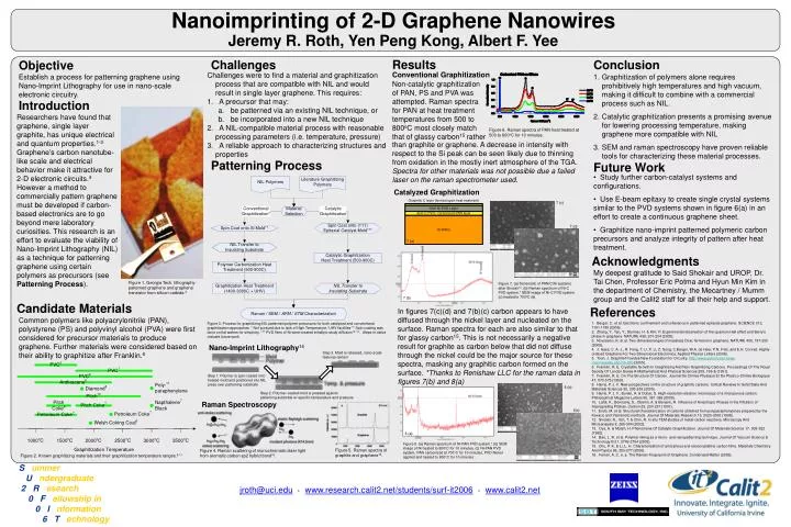
Results. Challenges. Conclusion. Objective. Conventional Graphitization. Challenges were to find a material and graphitization process that are compatible with NIL and would result in single layer graphene. This requires: A precursor that may:

E N D
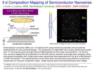
Results Challenges Conclusion Objective Conventional Graphitization • Challenges were to find a material and graphitization process that are compatible with NIL and would result in single layer graphene. This requires: • A precursor that may: • be patterned via an existing NIL technique, or • be incorporated into a new NIL technique • A NIL-compatible material process with reasonable processing parameters (i.e. temperature, pressure) • A reliable approach to characterizing structures and properties Establish a process for patterning graphene using Nano-Imprint Lithography for use in nano-scale electronic circuitry. • Graphitization of polymers alone requires prohibitively high temperatures and high vacuum, making it difficult to combine with a commercial process such as NIL. • Catalytic graphitization presents a promising avenue for lowering processing temperature, making graphene more compatible with NIL • SEM and raman spectroscopy have proven reliable tools for characterizing these material processes. Non-catalytic graphitization of PAN, PS and PVA was attempted. Raman spectra for PAN at heat treatment temperatures from 500 to 800oC most closely match that of glassy carbon15 rather Nanoimprinting of 2-D Graphene Nanowires Introduction Researchers have found that graphene, single layer graphite, has unique electrical and quantum properties.1-3 Graphene’s carbon nanotube-like scale and electrical behavior make it attractive for 2-D electronic circuits.4 However a method to commercially pattern graphene must be developed if carbon-based electronics are to go beyond mere laboratory curiosities. This research is an effort to evaluate the viability of Nano-Imprint Lithography (NIL) as a technique for patterning graphene using certain polymers as precursors (see PatterningProcess). Figure 6. Raman spectra of PAN heat treated at 500 to 800oC for 10 minutes. than graphite or graphene. A decrease in intensity with respect to the Si peak can be seen likely due to thinning from oxidation in the mostly inert atmosphere of the TGA. Spectra for other materials was not possible due a failed laser on the raman spectrometer used. Patterning Process Future Work • Study further carbon-catalyst systems and configurations. • Use E-beam epitaxy to create single crystal systems similar to the PVD systems shown in figure 6(a) in an effort to create a continuous graphene sheet. • Graphitize nano-imprint patterned polymeric carbon precursors and analyze integrity of pattern after heat treatment. Catalyzed Graphitization 7 (c) 7 (d) 7 (a) Acknowledgments My deepest gratitude to Said Shokair and UROP, Dr. Tai Chen, Professor Eric Potma and Hyun Min Kim in the department of Chemistry, the Mecartney / Mumm group and the Calit2 staff for all their help and support. Jeremy R. Roth, Yen Peng Kong, Albert F. Yee Figure 1. Georgia Tech. lithography-patterned graphene and graphene transistor from silicon carbide.5 Figure 7. (a) Schematic of PAN/C:Ni systems after Sinclair12. (b) Raman spectrum of Ni-C PVD system.* SEM image of Ni-C PVD system (c) heated to 700oC (d). 7 (b) Candidate Materials References In figures 7(c)(d) and 7(b)(c) carbon appears to have diffused through the nickel layer and nucleated on the surface. Raman spectra for each are also similar to that for glassy carbon15. This is not necessarily a negative result for graphite as carbon below that did not diffuse through the nickel could be the major source for these spectra, masking any graphitic carbon formed on the surface. *Thanks to Renishaw LLC for the raman data in figures 7(b) and 8(a) Common polymers like polyacrylonitrile (PAN), polystyrene (PS) and polyvinyl alcohol (PVA) were first considered for precursor materials to produce graphene. Further materials were considered based on their ability to graphitize after Franklin.6 1. Berger, C. et al. Electronic confinement and coherence in patterned epitaxial graphene. SCIENCE 312, 1191-1196 (2006). 2. Zhang, Y., Tan, Y., Stormer, H. & Kim, P. Experimental observation of the quantum Hall effect and Berry's phase in graphene. NATURE 438, 201-204 (2005). 3. Novoselov, K. et al. Two-dimensional gas of massless Dirac fermions in graphene. NATURE 438, 197-200 (2005). 4. J. Hass, C. A. J., R. Feng, T. Li, X. Li, Z. Song, C.Berger, W.A. de Heer, P.N. First, and E.H. Conrad. Highly-ordered Graphene For Two Dimensional Electronics. Applied Physics Letters (2006). 5. Toon, J. Graphite Provides New Foundation for Circuitry. http://www.gatech.edu/news-room/release.php?id=890 (2005). 6. Franklin, R. E. Crystallite Growth In Graphitizing And Non-Graphitizing Carbons. Proceedings Of The Royal Society Of London Series A-Mathematical And Physical Sciences 209, 196-& (1951). 7. Franklin, R. E. On The Structure Of Carbon. Journal De Chimie Physique Et De Physico-Chimie Biologique 47, 573-575 (1950). 8. Harris, P. J. F. New perspectives on the structure of graphitic carbons. Critical Reviews In Solid State And Materials Sciences 30, 235-253 (2005). 9. Harris, P. J. F., Burian, A. & Duber, S. High-resolution electron microscopy of a microporous carbon. Philosophical Magazine Letters 80, 381-386 (2000). 10. Lafdi, K., Bonnamy, S., Oberlin, A. & Benaim, R. Influence of Anisotropic Phases in the Filtration of Impregnating Pitches. Carbon 29, 233-237 (1991). 11. Endo, M. et al. Structural characterization of carbons obtained from polyparaphenylenes prepared by the Kovacic and Yamamoto methods. Journal Of Materials Research 13, 2023-2030 (1998). 12. Sinclair, R., Itoh, T. & Chin, R. In situ TEM studies of metal-carbon reactions. Microscopy And Microanalysis 8, 288-304 (2002). 13. Oya, A. & Marsh, H. Phenomena Of Catalytic Graphitization. Journal Of Materials Science 17, 309-322 (1982). 14. Bao, L. R. et al. Polymer inking as a micro- and nanopatterning technique. Journal Of Vacuum Science & Technology B 21, 2749-2754 (2003). 15. Chu, P. K. & Li, L. H. Characterization of amorphous and nanocrystalline carbon films. Materials Chemistry And Physics 96, 253-277 (2006). 16. Ferrari, A. C. e. a. The Raman Fingerprint of Graphene. Condensed Matter (2006). Figure 3. Process for graphitizing NIL patterned polymer precursors for both catalyzed and conventional graphitization approaches. * Not pursued due to lack of High Temperature / UHV facilities ** Spin coating was done on flat wafers for simplicity. *** PVD films of Ni were created initiallyto study diffusion12, 13. Steps in italics indicate future work. Nano-Imprint Lithography14 Step 3. Mold is released, nano-scale features remain Step 1. Polymer is spin-coated onto treated mold and positioned into NIL press over patterning substrate 8 (b) Step 2. Polymer-coated mold is pressed against patterning substrate w/ specific temperature and pressure Raman Spectroscopy 8(c) 8 (a) Figure 8. (a) Raman spectrum of Ni-PAN PVD system.* (b) SEM image of Ni heated to 800oC for 10 minutes. (c) Ni-PAN PVD system, PAN carbonized at 700oC for 10 minutes, PVD Nickel applied and heated to 800oC for 10 minutes . Figure 5. Raman spectra of graphite and graphene16. Figure 4. Raman scattering of monochromatic laser light from aromatic carbon sp2 hybrid bond15. Figure 2. Known graphitizing materials and their graphitization temperature ranges.6-11 S ummer U ndergraduate 2R esearch 0F ellowship in 0I nformation6T echnology jroth@uci.edu·www.research.calit2.net/students/surf-it2006·www.calit2.net