Download
1 / 54
540 likes | 666 Views
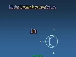
Bipolar Junction Transistors (BJT) Tai-Cheng Lee Electrical Engineering/GIEE, NTU. Why BJT. Application. Device Structure. Operation in Active Mode-(1). Operation in Active Mode-(2). Profile of minority carrier concentration. Operation in Active Mode-(3). Collector current.

E N D
Bipolar Junction Transistors (BJT) Tai-Cheng Lee Electrical Engineering/GIEE, NTU
Why BJT • Application
Operation in Active Mode-(2) • Profile of minority carrier concentration
Operation in Active Mode-(3) • Collector current
Operation in Active Mode-(4) • Base current
Operation in Active Mode-(4) • Emitter current
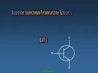
Structure of Actual Transistor • Equivalent circuit model for reverse active
Ebers-Moll (EM) Model-(1) • Universal model for BJT
Ebers-Moll (EM) Model-(2) • iC –vCB characteristic of an npn transistor
Current-Voltage Characteristics-(2) • Graphical representation • Thermal effect
Early Effect • Large-signal circuit model
Common-Emitter Characteristics –(2) • Saturation voltage VCEsat
Common-Emitter Characteristics –(3) • Saturation resistance RCEsat
Common-Emitter Characteristics –(4) • Analyze by E-M Model • Breakdown voltage
BJT Amplifier and Switch-(1) • Large-Signal operation
BJT Amplifier and Switch-(2) • Graphical analysis
BJT Amplifier and Switch-(3) • Operation as a switch
BJT Circuits at DC-(1) • Example 5.4
BJT Circuits at DC-(2) • Example 5.5
BJT Circuits at DC-(3) • Example 5.6
BJT Circuits at DC-(4) • Example 5.12
Biasing BJT -(1) • Fixed VBE
Biasing BJT -(2) • Classical discrete-circuit bias arrangement
Biasing BJT -(3) • Two power supplies • Collector-to-base feedback
Biasing BJT -(4) • By a constant current source
Small-Signal Operation-(1) • BJT Amplifier
Small-Signal Operation-(2) • Collector current and transconductance
Small-Signal Operation-(3) • Base current and the input resistance at base • Emitter current and the input resistance at emitter
Small-Signal Operation-(4) • Voltage gain
Small-Signal Models-(1) • DC and AC signal separation • Hybrid-p model
Small-Signal Models-(2) • T model
Small-Signal Models-(3) • Ex 5.14
Small-Signal Models-(4) • Perform small-signal analysis on the circuit schematic • Early Effect
Single-Stage BJT Amplifier-(1) • Basic structure
Single-Stage BJT Amplifier-(2) • Characterizing BJT Amplifier • Refer Table 5.5
Common-Emitter Amplifier-(1) • Small-signal model
Common-Emitter Amplifier with Emitter Resistance-(1) • Small-signal model
Common-Base Amplifier -(1) • Small-signal model