Download
1 / 25
310 likes | 833 Views
Chapter 9 output stages and power amplifiers . Introduction 9.1 Classification of output stages 9.2 Class A output stage 9.3 Class B output stage 9.4 Class AB output stage 9.5 Biasing the class AB circuit.

E N D
Chapter 9 output stages and power amplifiers Introduction 9.1 Classification of output stages 9.2 Class A output stage 9.3 Class B output stage 9.4 Class AB output stage 9.5 Biasing the class AB circuit
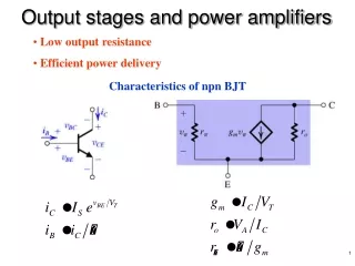
Small-signal approximation and models either are not applicable or must be used with care. THD (total harmonic distortion) Deliver the power to the load in efficient manner. Ex. To provide the amplifier with a low output resistance so that it can deliver the output signal to the load without loss of gain. Power dissipation is as low as possible. Power Amplifier
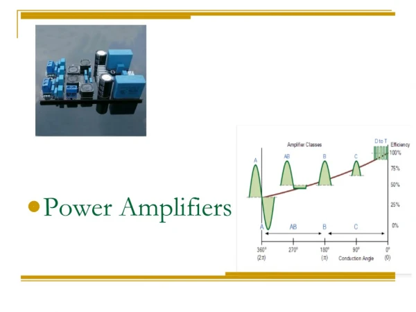
Power amplifiers are classified according to the collector current waveform that results when an input signal is applied. Conducting angle. Classification of Power Amplifier
Classification of Power Amplifier Collector current waveforms for transistors operating in (a) class A, (b) class B
Classification of Power Amplifier class AB class C
CE amplifier is not proper for using as a power amplifier DC supply power: ICQVcc , the area of ABCO Rc power: ICQURc, the area ofQBCD Collector dissipation power:ICQUCEQ, the area ofAQDO Load power:
Figure 14.3 Transfer characteristic of the emitter follower. This linear characteristic is obtained by neglecting the change in vBE1 with iL. The maximum positive output is determined by the saturation of Q1. In the negative direction, the limit of the linear region is determined either by Q1 turning off or by Q2 saturating, depending on the values of I and RL.
Figure 14.4 Maximum signal waveforms in the class A output stage of Fig. 14.2 under the condition I = VCC /RL or, equivalently, RL = VCC /I.
Class B Output Stage • A class B output stage. • Complementary circuits. • Push-pull operation • Maximum power-conversion efficiency is 78.5%
Class B Output Stage • When Vi=0, QN and Qp are cut off, Vo=0 • When Vi>0.5V, QN is on and Qp is cut off, Vo=Vi-VBEN • When Vi>0.5V, Qp is on and QN is cut off, Vo=Vi-VBEP
The load power Maximum load power Power –conversion efficiency
Power –conversion efficiency • Total supply power • Maximum total supply power
Power-conversion efficiency Maximum power-conversion efficiency Power –conversion efficiency
Power dissipation Maximum Power dissipation Power Dissipation
Power Dissipation • At the point of maximum power dissipation the efficiency can be evaluated:
A Class AB Output Stage Utilizing Diodes for Biasing The diode biasing has an Important advantage: Thermal stabilization of Quiescent current
A Class AB Output Stage Utilizing A VBE Multiplier for Biasing
May 25th, 2008 9.12; 9.13; 9.14; 9.15 Homework: