Download
1 / 36
360 likes | 449 Views
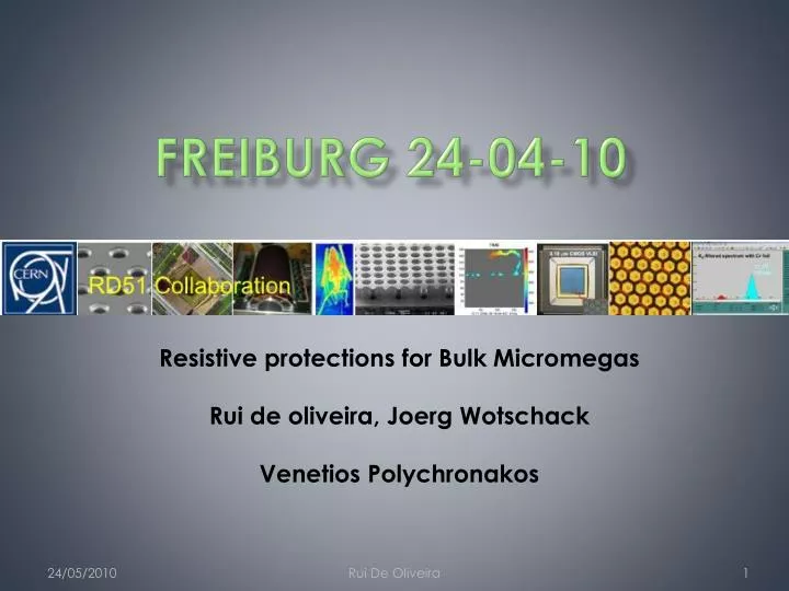
Freiburg 24-04-10. Resistive protections for Bulk Micromegas Rui de oliveira , Joerg Wotschack Venetios Polychronakos. Qualitative model of STD bulk and R11 read-out board. Aim Understand how it works Give a direction during R&D and prototype phase

E N D
Freiburg 24-04-10 Resistive protections for Bulk Micromegas Rui de oliveira, JoergWotschack VenetiosPolychronakos Rui De Oliveira
Qualitative model of STD bulk and R11 read-out board • Aim • Understand how it works • Give a direction during R&D and prototype phase • Help to define external components and their need • Predict the behavior in large detector The impedances are not treated as complex during this talk in order to get a model as easy as possible to understand. Rui De Oliveira
std detectors Mesh -580V Induced charge Gas gap 130um Strip 0.1mm x 10cm PCB 3mm 0 ohms c4 c2 c1 c3 GND R1 R3 C2 : in the range of 5pF Parasitic capacitor mesh to strip C3 : in the range of 1.5pF Parasitic capacitor strip to GND C4 : in the range of 4nF Parasitic capacitor mesh to GND R1 : ? 1M0hms Resistor to discharge strip R3 : ? Resistor for spark current limiting C1 : ? Spark current limiting Rui De Oliveira
Sparks std signals the rise time may be as quick as 0.7 ns, as defined by the new standard IEC 801-2:1991 (IEC 61000-4-2). Typical induced signal In a Micromegas detector Typical capacitor discharge current with a spark mechanism in a low resistive charge Rui De Oliveira
3 major frequencies “spark“ 1nS In the range of 1 GHz “Fast signal“ 10nS (electrons) In the range of 100 MHz “Slow signal” 100ns (Ions) In the range of 10 MHz All the signals are above 10 MHz Rui De Oliveira
Std BULK @ frequencies above 10MHz Z2 -580V Z1 5pF 1.5 pF C1 4nF Amp R1 R3 GND The power supply is a short at high frequencies And in any case 5pF serial to 4nF = 5pF Rui De Oliveira
@ frequencies above 10MHz Z2 Z1 5pF 1.5 pF C1 Amp R1 R3 Rui De Oliveira
@ frequencies above 10MHz Z2 Z1 5pF 1.5 pF C1 Amp R3 R1 5pf // 1.5pF 6.5pF Rui De Oliveira
@ frequencies above 10MHz Z2 Z1 6.5pF C1 Amp R3 R1 Impedance of 6.5pF above 10Mhz < 2500 Ohms R1 is above 1Mohms negligible influence Rui De Oliveira
@ frequencies above 10MHz Z2 Z1 6.5pF C1 Amp R3 Simplified equivalent schematic of one strip In a 100mm x 100mm detector for f > 10MHz Let’s look now at Z1 First the Amp Rui De Oliveira
Amplifier impedance 230 150 100 Ex: MICROROC Chip (being designed) input impedance (Thanks to RenaudGaglionne LAPP and LAL collaboration) Rui De Oliveira
Capacitor impedance Typical Capacitor impedance at High frequencies Ceramic capacitors NPO The smaller is the capacitor the better Is its behavior at high frequencies @ 10Mhz 100pF 200 Ohms @ 100Mhz 100pF 20 Ohms @ 1Ghz 100pf 4 Ohms Murata capacitor catalog Rui De Oliveira
@ 10MHz Ions Z2 Z1 6.5pF C1 Amp R3 R3 =10 Ohms C1= 200 pF 100 Ohms Amp 150 Ohms Total : 260 Ohms 6.5pF 2500 Ohms Rui De Oliveira
@ 10MHz Ions Z2 Z1 10% 90% 6.5pF C1 Amp R3 R3 =10 Ohms C1= 200 pF 100 Ohms Amp 150 Ohms Total : 260 Ohms 6.5pF 2500 Ohms (Value proportional to Detector size) Rui De Oliveira
@ 100MHz electrons Z2 Z1 6.5pF C1 Amp R3 R3 =10 Ohms C1= 200 pF 10Ohms !!!Amp 230 Ohms Total : 250 Ohms 6.5pF 250 Ohms Rui De Oliveira
@ 100MHz electrons Z2 Z1 50% 50% 6.5pF C1 Amp R3 R3 =10 Ohms C1= 200 pF 10Ohms !!!Amp 230 Ohms Total : 250 Ohms 6.5pF 250 Ohms Rui De Oliveira
Spark mode 1Ghz -580V spark Z1 Amp c3 c1 c4 c2 GND R1 R3 R1 is to high to drive any significant current Rui De Oliveira
Spark1GHz -580V spark Z1 Fast diodes c1 c4 c3 GND -C3 =1.5pF around 150 Ohms -C1 =200pF 2 Ohms -R3 = 10 Ohms -Diodes less than 1 Ohms R3 R -Peak current = 580V/13 Ohms 44Amps during a few ns - C1 and C3 are charged with C4 discharge C4 can not supply this current and maintain the mesh voltage Vmesh drops At one point the voltage between C4 and C1 is not enough to maintain the spark. The spark end and C4 is refill by the power supply through R. This RC4 constant define the dead time of the detector. (usually a few mS, all the detector is affected) Rui De Oliveira
Summary for 10cm x 10cm BULK • C1 in the range of 100 to 200pf (600V min) • Smaller : reduce detector efficiency but increase protection • Higher : increase spark current • R3 in the range of 10 to 20 Ohms • Higher : less efficiency for electrons • Less : higher spark current • Amp • Can we improve its impedance ! • Need protections for peaks currents in the range of 20 Amps during a few ns • Capacitance of the mesh • As low as possible (segmentation) to stop the spark fast • Parasitic capacitance of lines • As low as possible to reduce C1 and reduce sparks current. • As low as possible to avoid charge losses in the board. Rui De Oliveira
R11 Rui De Oliveira
R11 Embedded resistor 15 MOhms 5mm long PCB Resistive Strip 1MOhms for 1cm Copper Strip 0.15mm x 100mm GND Rui De Oliveira
R11 normal operation -580V Induced charge Strip 0.1mm x 10cm Copper Resistive strip Amp c2 c3 c5 c4 c6 GND R1 C2 : in the range of 5pF Parasitic capacitor mesh to strip C3 : in the range of 1.5pF Parasitic capacitor strip to GND C4 : in the range of 4nF Parasitic capacitor mesh to GND C5: ? Parasitic capacitor R-strip to GND C6: ? Parasitic capacitor R-strip to read-strip R1 : from 15 to 25 MOhms Resistor to discharge R-strip Rui De Oliveira
R11 normal operation above 10Mhz -580V Induced charge Strip 0.1mm x 10cm Copper R strip Amp c2 c3 c5 c4 c6 GND R1 -In normal operation the induced charge will be split first only between C5 and C6 - both sides of C6 and C5 capacitors are virtually grounded above 10MHz C6 on the mesh side is grounded at high frequencies with C4 C5 is grounded by the Amp (and also C3 assuming that C5<<C3 ) Rui De Oliveira
C5 /C6 ratio? mesh Gas Er1=1 Common Area=S=? h1=128um Resistive layer Coverlay Er2=4 h2=64um Strip c5 c6 C5 and C6 are sharing a common electrode in blue , this area is not known C5= Eo x Er2 x S/h2 C6= Eo x Er1x S/h1 C5/C6= Er2 x h1 / Er1 x h2 = 8 More than 90% of the charges will flow through C5 whatever is the value of the area Rui De Oliveira
R11 normal operation @ 10MHz Ions -580V 10% Strip 0.1mm x 10cm 90% c2 c3 c5 c4 c6 Amp 10% 80% GND Rui De Oliveira
R11 normal operation @ 100MHz electrons -580V 10% Strip 0.1mm x 10cm 90% c2 c3 c5 c4 c6 Amp 45% 45% GND Rui De Oliveira
R11 Sparks (1GHz) -580V spark 64 Strip 0.1mm x 10cm R strip oscilloscope c2 c3 c5 c4 c6 10pF GND 50 In the test 64 lines were connected together The oscilloscope probe has 10pF capacitance Rui De Oliveira
R11 Sparks (1GHz) -580V spark 64 Strip 0.1mm x 10cm R strip oscilloscope C3//C2 c5 c6 10pF 6.5pF x64 GND 50 Rui De Oliveira
R11 Sparks (1GHz) -580V spark 64 Strip 0.1mm x 10cm R strip oscilloscope C3//C2 c5 c6 10pF 6.5pF x64 V peak 0.5 ohms 0.4V 800mA 8mA 20mA GND 50 I peak in the 50 Ohms = 8mA I peak in C3//C2 x 64 = 800mA I peak in 10 pF= 20mA I peak in C5 in the range of 800mA Rui De Oliveira
C5 value? The impedance of 64 x (C3//C2) // 50ohms// 10pF is less than 1 ohm @1Ghz So during ‘mild sparks’ C5 see the full voltage 580V ZC5 @1Ghz is in the range of 580V/ 800mA 725ohms C5 in the range of 0.4pF Rui De Oliveira
R5 and R11 behaviordifference ? Rui De Oliveira
R5 0.2pF capacity from pad to line. Microvia Pad : 150um x 1.5mm 40um Kapton >1kv breakdown voltage Copper Strip 0.1mm x 100mm 1 mm long resistor More than 1kv breakdown Voltage (2 Kohms) R5 shows Higher gains than STD Bulk detectors ? Rui De Oliveira
Why a so big difference during sparks between R5 and R11 • R5 pad capacity to strip 0.2pF • R11 local capacity to strip 0.4pF • R5 discharge resistor 2KOhms • R11 discharge resistor 15MOhms • R5 spark currents power supply limitation • R11 spark currents a few nA in average • We have some ideas to explain this effect but need some more measurements to be sure. It will also explain why: • R5 shows higher gains than Std Bulk • R11 has15us extra signal after spark Rui De Oliveira
C4 Value? • C4 (mesh capacity) value has no importance in normal operation • During ‘mild sparks’ C4 should only charge C5 • C4 voltage drops during ‘mild sparks’ should not induce a charge to each strips bigger than 1000e- • We still need to define precisely C4 ( uF range) • But we have no limitation on C4, we do not need to segment the mesh. Rui De Oliveira
Spark V on the 50Ohms Time No resonances no big inductive effects Should we adapt the lines to the amplifier? There is some signs of reflection Rui De Oliveira
Conclusion • We still need to understandthe R5 and R11 difference • We need to define the optimum value of C4 in R11 detector • We can start to predict the effect of the size on the detector behavior • We are building now 2 new small detectors to: • Increase the statistics • Improve our understanding • See if we can reduce again the ‘mild spark’ currents • We have also started to design a large size version of R11 Rui De Oliveira