Download
1 / 103
1.09k likes | 1.35k Views
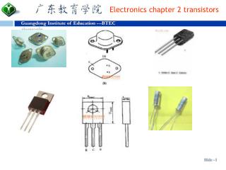
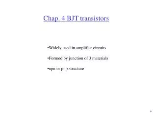
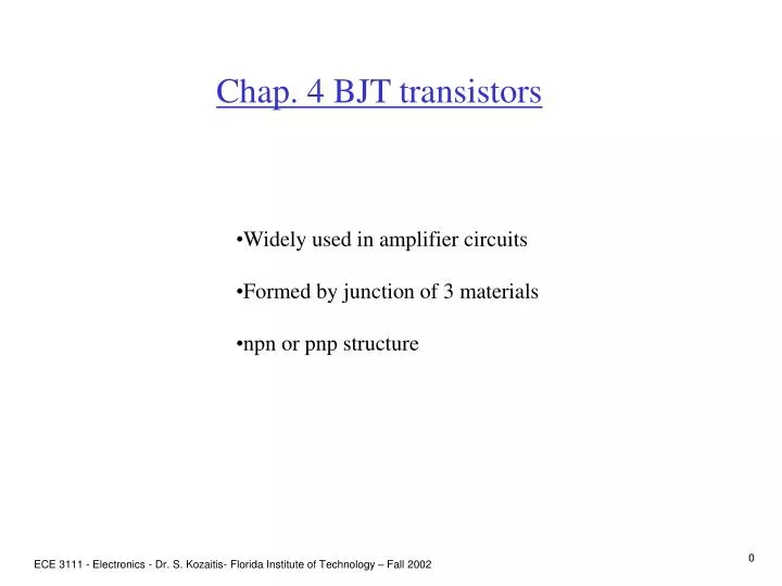
Chap. 4 BJT transistors. Widely used in amplifier circuits Formed by junction of 3 materials npn or pnp structure. pnp transistor. Operation of npn transistor. Large current. Modes of operation of a BJT transistor. Mode BE junction BC junction cutoff reverse biased reverse biased

E N D
Chap. 4 BJT transistors • Widely used in amplifier circuits • Formed by junction of 3 materials • npn or pnp structure ECE 3111 - Electronics - Dr. S. Kozaitis- Florida Institute of Technology – Fall 2002
ECE 3111 - Electronics - Dr. S. Kozaitis- Florida Institute of Technology – Fall 2002
pnp transistor ECE 3111 - Electronics - Dr. S. Kozaitis- Florida Institute of Technology – Fall 2002
ECE 3111 - Electronics - Dr. S. Kozaitis- Florida Institute of Technology – Fall 2002
ECE 3111 - Electronics - Dr. S. Kozaitis- Florida Institute of Technology – Fall 2002
Operation of npn transistor Large current ECE 3111 - Electronics - Dr. S. Kozaitis- Florida Institute of Technology – Fall 2002
Modes of operation of a BJT transistor Mode BE junction BC junction cutoff reverse biased reverse biased linear(active) forward biased reverse biased saturation forward biased forward biased ECE 3111 - Electronics - Dr. S. Kozaitis- Florida Institute of Technology – Fall 2002
Summary of npn transistor behavior npn IC collector base large current IB + VBE - emitter IE small current ECE 3111 - Electronics - Dr. S. Kozaitis- Florida Institute of Technology – Fall 2002
Summary of pnp transistor behavior pnp IC collector base large current IB + VBE - emitter IE small current ECE 3111 - Electronics - Dr. S. Kozaitis- Florida Institute of Technology – Fall 2002
Summary of equations for a BJT IE IC IC=bIB b is the current gain of the transistor 100 VBE = 0.7V(npn) VBE = -0.7V(pnp) ECE 3111 - Electronics - Dr. S. Kozaitis- Florida Institute of Technology – Fall 2002
4.5 Graphical representation of transistor characteristics IC IB Output circuit Input circuit IE ECE 3111 - Electronics - Dr. S. Kozaitis- Florida Institute of Technology – Fall 2002
Input characteristics IB IB VBE 0.7V • Acts as a diode • VBE0.7V ECE 3111 - Electronics - Dr. S. Kozaitis- Florida Institute of Technology – Fall 2002
Output characteristics IC IB = 40mA IC IB = 30mA IB = 20mA IB = 10mA VCE Early voltage Cutoff region • At a fixed IB, IC is not dependent on VCE • Slope of output characteristics in linear region is near 0 (scale exaggerated) ECE 3111 - Electronics - Dr. S. Kozaitis- Florida Institute of Technology – Fall 2002
Biasing a transistor • We must operate the transistor in the linear region. • A transistor’s operating point (Q-point) is defined by • IC, VCE, and IB. ECE 3111 - Electronics - Dr. S. Kozaitis- Florida Institute of Technology – Fall 2002
4.6 Analysis of transistor circuits at DC For all circuits: assume transistor operates in linear region write B-E voltage loop write C-E voltage loop Example 4.2 B-E junction acts like a diode VE = VB - VBE = 4V - 0.7V = 3.3V IC IE = (VE - 0)/RE = 3.3/3.3K = 1mA IC IE = 1mA VC = 10 - ICRC = 10 - 1(4.7) = 5.3V IE ECE 3111 - Electronics - Dr. S. Kozaitis- Florida Institute of Technology – Fall 2002
Example 4.6 B-E Voltage loop 5 = IBRB + VBE, solve forIB IB = (5 - VBE)/RB = (5-.7)/100k = 0.043mA IC= bIB = (100)0.043mA = 4.3mA VC = 10 - ICRC = 10 - 4.3(2) = 1.4V b = 100 IC IB IE ECE 3111 - Electronics - Dr. S. Kozaitis- Florida Institute of Technology – Fall 2002
Exercise 4.8 VE = 0 - .7 = - 0.7V b = 50 IE = (VE - -10)/RE = (-.7 +10)/10K = 0.93mA IC IE = 0.93mA IB= IC/b = .93mA/50 = 18.6mA VC = 10 - ICRC = 10 - .93(5) = 5.35V VCE = 5.35 - -0.7 = 6.05V IC IB IE ECE 3111 - Electronics - Dr. S. Kozaitis- Florida Institute of Technology – Fall 2002
Summary of npn transistor behavior npn IC collector base large current IB + VBE - emitter IE small current ECE 3111 - Electronics - Dr. S. Kozaitis- Florida Institute of Technology – Fall 2002
Summary of equations for a BJT IE IC IC=bIB b is the current gain of the transistor 100 VBE = 0.7V(npn) VBE = -0.7V(pnp) ECE 3111 - Electronics - Dr. S. Kozaitis- Florida Institute of Technology – Fall 2002
Prob. 4.32 • Use a voltage divider, RB1 and RB2 to bias VB to avoid two power supplies. • Make the current in the voltage divider about 10 times IB to simplify the analysis. Use VB = 3V and I = 0.2mA. (a) RB1 and RB2 form a voltage divider. Assume I >> IB I = VCC/(RB1 + RB2) .2mA = 9 /(RB1 + RB2) AND VB = VCC[RB2/(RB1 + RB2)] 3 = 9 [RB2/(RB1 + RB2)], Solve for RB1 and RB2. RB1 = 30KW, and RB2 = 15KW. I IB ECE 3111 - Electronics - Dr. S. Kozaitis- Florida Institute of Technology – Fall 2002
Prob. 4.32 • Find the operating point • Use the Thevenin equivalent circuit for the base • Makes the circuit simpler • VBB = VB = 3V • RBB is measured with voltage sources grounded • RBB = RB1|| RB2= 30KW || 15KW = . 10KW ECE 3111 - Electronics - Dr. S. Kozaitis- Florida Institute of Technology – Fall 2002
Prob. 4.32 Write B-E loop and C-E loop B-E loop VBB = IBRBB + VBE +IERE C-E loop VCC = ICRC + VCE +IERE Solve for,IC, VCE, and IB. This is how all DC circuits are analyzed and designed! C-E loop B-E loop ECE 3111 - Electronics - Dr. S. Kozaitis- Florida Institute of Technology – Fall 2002
Example 4.8 • 2-stage amplifier, 1st stage has an npn transistor; 2nd stage has an pnp transistor. • IC = bIB • IC IE • VBE = 0.7(npn) = -0.7(pnp) • b = 100 • Find IC1, IC2, VCE1, VCE2 • Use Thevenin circuits. ECE 3111 - Electronics - Dr. S. Kozaitis- Florida Institute of Technology – Fall 2002
Example 4.8 • RBB1 = RB1||RB2 = 33K • VBB1 = VCC[RB2/(RB1+RB2)] • VBB1 = 15[50K/150K] = 5V • Stage 1 • B-E loop • VBB1 = IB1RBB1 + VBE +IE1RE1 • Use IB1 IE1/ b • 5 = IE133K/ 100 + .7 + IE13K • IE1 = 1.3mA IB1 IE1 ECE 3111 - Electronics - Dr. S. Kozaitis- Florida Institute of Technology – Fall 2002
Example 4.8 C-E loop neglect IB2 because it is IB2 << IC1 VCC = IC1RC1 + VCE1 +IE1RE1 15 = 1.3(5) + VCE1 +1.3(3) VCE1= 4.87V IC1 IE1 ECE 3111 - Electronics - Dr. S. Kozaitis- Florida Institute of Technology – Fall 2002
Example 4.8 • Stage 2 • B-E loop IE2 VCC = IE2RE2 + VEB +IB2RBB2 + VBB2 15 = IE2(2K) + .7 +IB2 (5K)+ 4.87 + 1.3(3) Use IB2 IE2/ b, solve for IE2 IE2 = 2.8mA IB2 ECE 3111 - Electronics - Dr. S. Kozaitis- Florida Institute of Technology – Fall 2002
Example 4.8 • Stage 2 • C-E loop IE2 VCC = IE2RE2 + VEC2 +IC2RC2 15 = 2.8(2) + VEC2 + 2.8(2.7) solve for VEC2 VCE2 = 1.84V IC2 ECE 3111 - Electronics - Dr. S. Kozaitis- Florida Institute of Technology – Fall 2002
Summary of DC problem • Bias transistors so that they operate in the linear region B-E junction forward biased, C-E junction reversed biased • Use VBE = 0.7 (npn), IC IE, IC = bIB • Represent base portion of circuit by the Thevenin circuit • Write B-E, and C-E voltage loops. • For analysis, solve for IC, and VCE. • For design, solve for resistor values (IC and VCE specified). ECE 3111 - Electronics - Dr. S. Kozaitis- Florida Institute of Technology – Fall 2002
4.7 Transistor as an amplifier • Transistor circuits are analyzed and designed in terms of DC and ac versions of the same circuit. • An ac signal is usually superimposed on the DC circuit. • The location of the operating point (values of IC and VCE) of the transistor affects the ac operation of the circuit. • There are at least two ac parameters determined from DC quantities. ECE 3111 - Electronics - Dr. S. Kozaitis- Florida Institute of Technology – Fall 2002
Transconductance IB ac output signal DC output signal A small ac signal vbe is superimposed on the DC voltage VBE. It gives rise to a collector signal current ic, superimposed on the dc current IC. (DC input signal 0.7V) The slope of the ic - vBE curve at the bias point Q is the transconductance gm: the amount of ac current produced by an ac voltage. ac input signal ECE 3111 - Electronics - Dr. S. Kozaitis- Florida Institute of Technology – Fall 2002
Transconductance Transconductance = slope at Q point gm = dic/dvBE|ic = ICQ where IC = IS[exp(-VBE/VT)-1]; the equation for a diode. ac output signal DC output signal gm = ISexp(-VBE/VT) (1/VT) gm IC/VT (A/V) DC input signal (0.7V) ac input signal ECE 3111 - Electronics - Dr. S. Kozaitis- Florida Institute of Technology – Fall 2002
ac input resistance of transistor IB ac output signal DC output signal ac input resistance 1/slope at Q point rp = dvBE/dib|ic = ICQ rp VT /IB re VT /IE DC input signal (0.7V) ac input signal ECE 3111 - Electronics - Dr. S. Kozaitis- Florida Institute of Technology – Fall 2002
4.8 Small-signal equivalent circuit models • ac model • Hybrid-p model • They are equivalent • Works in linear region only ECE 3111 - Electronics - Dr. S. Kozaitis- Florida Institute of Technology – Fall 2002
Steps to analyze a transistor circuit 1 DC problem Set ac sources to zero, solve for DC quantities, IC and VCE. 2 Determine ac quantities from DC parameters Find gm, rp, and re. 3 ac problem Set DC sources to zero, replace transistor by hybrid-p model, find ac quantites, Rin, Rout, Av, and Ai. ECE 3111 - Electronics - Dr. S. Kozaitis- Florida Institute of Technology – Fall 2002
Example 4.9 Find vout/vin, (b = 100) DC problem Short vi, determine IC and VCE B-E voltage loop 3 = IBRB + VBE IB = (3 - .7)/RB = 0.023mA C-E voltage loop VCE = 10 - ICRC VCE = 10 - (2.3)(3) VCE = 3.1V Q point: VCE = 3.1V, IC =2.3mA ECE 3111 - Electronics - Dr. S. Kozaitis- Florida Institute of Technology – Fall 2002
Example 4.9 b c + vout - + vbe - e ac problem Short DC sources, input and output circuits are separate, only coupled mathematically gm = IC/VT = 2.3mA/25mV = 92mA/V rp = VT/ IB = 25mV/.023mA = 1.1K vbe= vi [rp / (100K + rp)] = 0.011vi vout = - gm vbeRC vout = - 92(0.011vi)3K vout/vi = -3.04 ECE 3111 - Electronics - Dr. S. Kozaitis- Florida Institute of Technology – Fall 2002
Exercise 4.24 (a) Find VC, VB, and VE, given: b = 100, VA = 100V IE = 1 mA IB IE/b= 0.01mA VB = 0 - IB10K = -0.1V VE = VB - VBE = -0.1 - 0.7 = -0.8V VC = 10V - IC8K = 10 - 1(8) = 2V VB ECE 3111 - Electronics - Dr. S. Kozaitis- Florida Institute of Technology – Fall 2002
Exercise 4.24 (b) Find gm, rp, and r0, given: b = 100, VA = 100V gm = IC/VT = 1 mA/25mV = 40 mA/V rp = VT/ IB = 25mV/.01mA = 2.5K r0 = output resistance of transistor r0 = 1/slope of transistor output characteristics r0 = | VA|/IC = 100K ECE 3111 - Electronics - Dr. S. Kozaitis- Florida Institute of Technology – Fall 2002
Summary of transistor analysis • Transistor circuits are analyzed and designed in terms of DC and ac versions of the same circuit. • An ac signal is usually superimposed on the DC circuit. • The location of the operating point (values of IC and VCE) of the transistor affects the ac operation of the circuit. • There are at least two ac parameters determined from DC quantities. ECE 3111 - Electronics - Dr. S. Kozaitis- Florida Institute of Technology – Fall 2002
Steps to analyze a transistor circuit 1 DC problem Set ac sources to zero, solve for DC quantities, IC and VCE. 2 Determine ac quantities from DC parameters Find gm, rp, and ro. 3 ac problem Set DC sources to zero, replace transistor by hybrid-p model, find ac quantites, Rin, Rout, Av, and Ai. ro ECE 3111 - Electronics - Dr. S. Kozaitis- Florida Institute of Technology – Fall 2002
Circuit from Exercise 4.24 + Vout - IE = 1 mA VC = 10V - IC8K = 10 - 1(8) = 2V IB IE/b= 0.01mA gm = IC/VT = 1 mA/25mV = 40 mA/V VB = 0 - IB10K = -0.1V rp = VT/ IB = 25mV/.01mA = 2.5K VE = VB - VBE = -0.1 - 0.7 = -0.8V ECE 3111 - Electronics - Dr. S. Kozaitis- Florida Institute of Technology – Fall 2002
ac equivalent circuit b c + vout - e NeglectingRo vout = -(gmvbe)(Rc ||RL) Av =vout/vi = - 80 vbe = (Rb||Rpi)/ [(Rb||Rpi) +Rs]vi vbe = 0.5vi vout = -(gmvbe)(Ro||Rc ||RL) vout = -154vbe Av =vout/vi = - 77 ECE 3111 - Electronics - Dr. S. Kozaitis- Florida Institute of Technology – Fall 2002
Prob. 4.76 b=100 + Vout - ECE 3111 - Electronics - Dr. S. Kozaitis- Florida Institute of Technology – Fall 2002
Prob. 4.76 b c + Vout - ib e = bib Rin Rout (a) Find Rin Rin = Rpi = VT/IB = (25mV)100/.1 = 2.5KW (c) Find Rout Rout = Rc = 47KW (b) Find Av = vout/vin vout= - bibRc vin= ib(R +Rpi) Av = vout/vin = - bibRc/ ib(R +Rpi ) = - bRc/(R +Rpi) = - 100(47K)/(100K +2.5K) = - 37.6 ECE 3111 - Electronics - Dr. S. Kozaitis- Florida Institute of Technology – Fall 2002
4.9 Graphical analysis Input circuit B-E voltage loop VBB = IBRB +VBE IB = (VBB - VBE)/RB ECE 3111 - Electronics - Dr. S. Kozaitis- Florida Institute of Technology – Fall 2002
Graphical construction of IB and VBE IB = (VBB - VBE)/RB If VBE = 0, IB = VBB/RB If IB = 0, VBE = VBB VBB/RB ECE 3111 - Electronics - Dr. S. Kozaitis- Florida Institute of Technology – Fall 2002
Load line Output circuit C-E voltage loop VCC = ICRC +VCE IC = (VCC - VCE)/RC ECE 3111 - Electronics - Dr. S. Kozaitis- Florida Institute of Technology – Fall 2002
Graphical construction of IC and VCE IC = (VCC - VCE)/RC If VCE = 0, IC = VCC/RC If IC = 0, VCE = VCC VCC/RC ECE 3111 - Electronics - Dr. S. Kozaitis- Florida Institute of Technology – Fall 2002
Graphical analysis Input signal Output signal ECE 3111 - Electronics - Dr. S. Kozaitis- Florida Institute of Technology – Fall 2002
Bias point location effects • Load-line A results in bias point QA which is too close to VCC and thus limits the positive swing of vCE. • Load-line B results in an operating point too close to the saturation region, thus limiting the negative swing of vCE. ECE 3111 - Electronics - Dr. S. Kozaitis- Florida Institute of Technology – Fall 2002