Download
1 / 14
140 likes | 297 Views
James Leaver, Imperial College, IOP HEPP Conference 2005. The CMS Tracker Front End Readout Electronics. Contents:. The Compact Muon Solenoid and Silicon Tracker readout system The CMS Tracker Front End Driver Production testing of the FED Testing FED performance in the Lab Summary.

E N D
James Leaver, Imperial College, IOP HEPP Conference 2005 The CMS Tracker Front End Readout Electronics Contents: • The Compact Muon Solenoid and Silicon Tracker readout system • The CMS Tracker Front End Driver • Production testing of the FED • Testing FED performance in the Lab • Summary Imperial College James Leaver
General purpose detector for the CERN LHC Designed to study p-p (14 TeV CM energy) & Pb-Pb collisions (1.3 PeV CM energy) Particle bunches cross at 40 MHz 109 Hz interaction rate at p-p luminosity (1034cm-2s-1) 100 Hz of interactions recorded (data reducing trigger system) The Compact Muon Solenoid • Design goals: • A high performance redundant Muon system • The best possible Electromagnetic Calorimeter • A hermetic Hadron Calorimeter with good energy resolution • A high quality central Tracking system Based upon a 4T solenoidal magnet – the largest ever built Solenoid Solenoid is so large that all tracking devices & calorimetry can be placed inside Compact Emphasis on detecting Muons (Muons expected to provide clean signatures for a wide range of physics processes, e.g. H→ZZ(*)→4μ) Muon Imperial College James Leaver
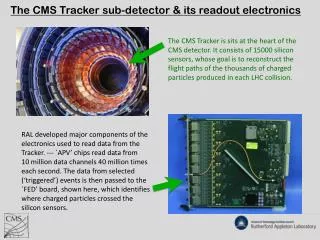
9 million detector channels 73,000 APV25 readout chips Each APV samples 128 channels at 40 MHz Data output when APV receives L1A signal from Trigger Control System Analog data transmitted optically via 100m links to Front End Drivers in counting room 43,000 optical readout links 1.3 TB/s @ 100 kHz L1As 440 FEDs FED reduces immense data volume to level with which the CMS DAQ can cope APV readout chip DCU 128:1 APV MUX 2:1 APV readout chip 128:1 PLL Front End Module Detector ADC FPGA x12 ADC Silicon Tracker Readout System Optical Tx On Detector: High Radiation x96 FED To CMS DAQ x8 FPGA ADC FPGA x12 ADC RAM Imperial College James Leaver
The Front End Driver FE data processing FPGA VME FPGA BE FPGA Opto RX • Input = 96 optical fibres, each from a MUX’ed pair of APVs • Input data rate = ~3.4 GB/s • 8 Front End Units perform data reduction (‘Zero Suppression’) • Back End FPGA collects FE data & builds events • Events output using Slink 64 protocol (high-capacity link) • Output data rate = ~50 Mb/s per % of Tracker occupancy High density, high performance board, at the cutting edge of PCB design 1 FE Unit Power Slink Imperial College James Leaver
The FED Front-End Optical Optical to electrical Analog to 10bit digital Cluster finding Clock phase To extract hit information, need: • Data Synchronization and reordering • Pedestal subtraction • Common mode noise subtraction • Cluster (hit) finding Opto RX, 12 way 3 x Delay FPGA (ADC clk timing) Virtex II, 2M gate FPGA performs signal processing Optical ribbon cable input Analog circuitry duplicated on secondary side 6 x Dual 40MHz, 10bit ADCs 12 x Buffers Example De-MUX’ed APV Data Frame Digital header (Pipeline address + error bits) 128 analog values (one for each channel) Signal magnitude → MIP Imperial College James Leaver
FED Production Testing 0. Quality Controls during Assemblyprocess AOI, X-ray • Essential to catch manufacturing errors as soon as possible • Detailed custom test procedure at Assembly Plant • Plant operatives require user-friendly FED Acceptance Testing Software 1. Custom Tests at Assembly PlantBScan, VME crate 2. Tests at RAL & ICOptoRx, Full crate Manual testing by Assembly Plant operatives Boundary Scan testing for digital connectivity + VME Crate Testing for Digital & Analog functionality, using custom software suite 3. Tests at CERN Prevessin 904Readout Integration 4. Installation at CMS USC55 Test Flow from Assembly Plant to USC55. 500 boards to test over 10 months Imperial College James Leaver
Acceptance Testing Software • Simple push-button controls • Fully automated testing of digital functionality & analog readout path • Automated generation of XML/HTML results database Example Test Page (12 pages in total) Example Results Pages Imperial College James Leaver
FED Production Timeline 2003 –Q1 Manufacture first 2 FEDv1s - Initial testing Express/SAETech 2003 –Q2 Manufacture 3 more FEDv1s Express/SAETech 2003 –Q4 Manufacture 6 FEDv1s - Many serious manufacture errors Express/SAETech 2004 –Q1 Manufacture 6 FEDv1s - Complete tests of Prototype FEDv1 design DDi 2004 –Q2 Implement changes for FEDv2 and review 2004 –Q3 Manufacture first 2 FEDv2s - Dispatch calls for final manufacture quotes DDi 2004 –Q4 Test initial FEDv2s - Select DDi for final job; negotiate testing, schedules, etc. 2005 –Q1 Manufacture another 25 FEDv2s - Award contract for final job to DDi DDi 2005 –Q2 to 2006 – Q2 Manufacture 500 FEDs (~50 per month) - Fully test batches in UK - Re-test at CERN prior to CMS installation DDi (now eXception) Imperial College James Leaver
Laboratory Testing of the FED Testing the FED with optical input under realistic CMS conditions requires custom hardware: • Emulates Silicon Tracker optical data • Test data loaded via VME to on-board SRAMS • Data converted to analog via 3 DACs • 8 CMS Analog Optical Hybrids convert analog data to optical format & drive the FED • 24 Optical Outputs → 4 FED Testers required for one FED The FED Tester AOHs VME FPGA X-point switch System FPGA Optical outputs DACs Master & Slave I/O Power Imperial College James Leaver
Full System Tests Access VME with SBS620 PCI-VME link FT (slave) SBS Interface FT (slave) VME crate FT (slave) Generic PCI Card FT (master) J1 Connector J2 Connector Slink Rx Simulate Local Trigger Control System Merge 96 fibres into 8 ribbons of 12 fibres Slink PC (PCI-X slots) LVDS cable J0 Connector Throttle signals from FED to FT Slink Tx Clock & L1As from FT to FED Transition Card FED Imperial College James Leaver
Comprehensive test suit built around core framework – have verified that: Every input detector hit is correctly identified (under realistic CMS conditions) FED channel noise is < 1 ADC count FED inter-channel crosstalk is < 1% of signal amplitude on neighbouring channels (next-nearest neighbours unaffected) Extensive software development: One function to calibrate, configure & initialise entire system One object to access all hardware & software elements Supports any number of FEDs & related hardware items (currently test one FED at a time) FED Tester Software Can perform rigorous error checking on billions of events, processed at highest CMS data rates Imperial College James Leaver
Mean = 2.96 strips per cluster Average size of hit = 1.91 bytes Measurement of Deadtime Vs Tracker Occupancy • 1 Slink receiver accepts data from 2 FEDs • Peak data rate = 400 MB/s • Assumed that each FED transmits equal data volume… • …But in practice, high & low occupancy FEDs will be paired Emulated CMS operating conditions: • Random 100 kHz triggers • Readout rate through Slink limited to maximum of 200 MB/s • Randomly generated events with simulated CMS cluster distribution sent to FED • Measured fraction of events vetoed by FED as a function of detector occupancy Simulated cluster distribution generated from the CMS-IN 2001/025 Note: “On Calibration, Zero Suppression Algorithms and Data Format for the Silicon Tracker FEDs” Imperial College James Leaver
Deadtime Vs Tracker Occupancy: Results L1As Vetoed Vs Tracker Occupancy • FED operates correctly under CMS conditions • Events lost when occupancy exceeds ~2.8% (@ 200 MB/s) At CMS - Smaller events (less padding) Peak data rate = 400 MB/s Expected occupancy ~1.7% Unlikely that any events will be lost during normal operation Imperial College James Leaver
Summary • The CMS Tracker Readout Electronics: • The FED is a vital component of the CMS Tracker • Provides the link between detector & CMS DAQ • FED Assembly: • Manufacturing schedule is on time • Rigorous testing procedures should ensure that manufacturing faults are discovered before FEDs leave the Assembly Plant, minimising potential delays • FED Performance Testing: • Framework in place for current and future FED testing procedures • FED has been successfully tested under realistic CMS operating conditions, no significant problems found Imperial College James Leaver