Download
1 / 22
220 likes | 229 Views
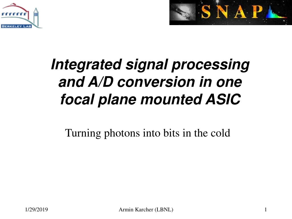
Turning photons into bits in the cold. Overview. What is the CRIC 2 chip ? Why did we build it ? How does it work ? Multi slope integrator ADC Test results Linearity Noise Cross-talk Power consumption AC-coupling Cold performance Where we go from here Conclusion.

E N D
Turning photons into bits in the cold Armin Karcher (LBNL)
Overview • What is the CRIC 2 chip ? • Why did we build it ? • How does it work ? • Multi slope integrator • ADC • Test results • Linearity • Noise • Cross-talk • Power consumption • AC-coupling • Cold performance • Where we go from here • Conclusion Armin Karcher (LBNL)
CRIC 2: 4 Channel CCD readout Pre-Amp CDS Multi-slope 13 Bit ADC Logic I/O Voltage Reference Armin Karcher (LBNL)
Why did we build it? The CRIC 2 chip is part of a fully-integrated detector readout system for the proposed SNAP space telescope. Integrating many detectors on a passively cooled focal plane strongly favors local readout with a micro-power ASIC. Armin Karcher (LBNL)
Readout electronics goals • Low noise:Photometry: 2.8e rms (9.8mV) @100kHz • Large dynamic range:96dB from noise floor to 130ke well depth (16-bit) • Readout frequency: 100 kHz & 50kHz • Radiation tolerant: 10 kRad ionization (well shielded) • Low power:≈ 200mJ/image/channel ≈ 10mW/channel • Operation at 140K and 300KAllow normal operation at 140K and chip testing at room temperature • Compact • Robust, space qualified Armin Karcher (LBNL)
Signal Path • Voltage Reference • Auto Gain Multi Slope • Pipeline ADC Armin Karcher (LBNL)
Multi Slope Integrator Armin Karcher (LBNL)
Multi Slope Integrator • >16 bits of dynamic range with 13 bit ADC • Large signals are Poisson noise dominated • Charge is conserved (no offset) • Gain calibration at 3 points fully characterizes the system. Armin Karcher (LBNL)
ADC design Pipeline architecture • Low power • High resolution • Compact • 12 identical stages minimize layout effort • All capacitor design is radiation tolerant Armin Karcher (LBNL)
Integral Nonlinearity Armin Karcher (LBNL)
Integral Nonlinearity deviation from line fit Note: 1 LSB ≈ 1e- ≈ 3.5 mV Armin Karcher (LBNL)
Differential Nonlinearity Armin Karcher (LBNL)
Noise Gain 32: Multislope dominated noise Gain 2 Less than 1 bit RMS ADC noise ! Gain 1 Armin Karcher (LBNL)
Crosstalk • Crosstalk of less than 2 ADU for a full-scale signal. • This is at the measurement limit of our system. Armin Karcher (LBNL)
Power consumption • Bandgap Reference 0.86 mW • Reference Buffer 11.29 mW • ADC 22.84 mW • Preamp/Integrator 31.55 mW Total power less than 17 mW/channel Armin Karcher (LBNL)
AC Coupling Vref ClampR 200KW Chip input To CCD output stage Input amplifier On/off C=1uF Clamp Vref Clamp is on during start up (CCD power up) to charge C, off afterwards. During normal operation: ClampR is closed only during the CCD reset level integration. On/off is closed only during CCD reset and video level integration. Armin Karcher (LBNL)
AC Coupling performance • No observable change in gain • - DC coupled: • Gain = 3.5919 µV/ADU • - AC coupled: • Gain = 3.5916µV/ADU • No change in noise Armin Karcher (LBNL)
Voltage Reference Only 7mV variation in voltage during cooldown Armin Karcher (LBNL)
Cold Performance Noise at 298K: 2.23ADU Noise at 153K: 1.90ADU • Noise reduction of ~15% • Gain increase of ~5% Armin Karcher (LBNL)
Outlook • Integration of digital control and timing is in process. Look for the CRIC3 chip next spring. • Radiation testing is planned for this summer. • A clock driver and bias generator chip (CLIC) is being developed to create a fully integrated focal plane readout system. Armin Karcher (LBNL)
CLIC chip in development 0V, 80V adj (Vsub dc) -5V, +15V adj (V clk) -5V, +10V adj (TG clk) Power supply (4V?) -5V, +10V adj (H clk) CLIC 0V, +5V adj (Output gate dc) -8V, +8V adj (SW clk) -8V, 0V adj (Reset gate clk) -15V, 0V adj (Reset drain dc) Input clock -25V,0 DC adj (Output drain dc) -20V,0 DC (p+ guard dc) Config. data 3.3V/2.5V (Analog/Dig) CRIC dc Armin Karcher (LBNL)
Conclusion • Linearity is ~3.5µV (1 ADU) RMS • 6.5µV cold noise is well below system goal • Excellent crosstalk: -95dB • The CRIC2 CCD readout chip meets all design requirements! Armin Karcher (LBNL)