Download
1 / 34
340 likes | 497 Views
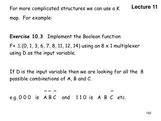
Lecture 11. For more complicated structures we can use a K map. For example: Exercise 10.3 Implement the Boolean function F = S (0, 1, 3, 6, 7, 8, 11, 12, 14) using an 8 x 1 multiplexer using D as the input variable.

E N D
Lecture 11 For more complicated structures we can use a K map. For example: Exercise 10.3 Implement the Boolean function F= S (0, 1, 3, 6, 7, 8, 11, 12, 14) using an 8 x 1 multiplexer using D as the input variable. If D is the input variable then we are looking for all the 8 possible combinations of A, B and C. e.g. 0 0 0 is A B C and 1 1 0 is A B C etc.
A B A B A B A B 1 1 1 C D 1 C D 1 1 1 C D 1 1 C D Step 1 Mark 1s in the appropriate square of the K map Step 2 Group together the 8 ABC terms and write out what the values of D and NOT D are
If both D and NOT D are present (1,1) then the data entry is 1 If neither D nor NOT D is present (0,0) then the data entry is 0 If only one entry is present (either (0,1) or (1,0)) (then term with 1 is the data entry)
Exercise 11.1 Redo the exercise 10.3 using A as the data inputs and B C D as the control lines. You can use the same K map. Show that the data entry values are (0-7): 1, NOT A, 0, 1, A, 0, 1 and NOT A
Exercise 11.2 Redo the exercise 10.3 using C and D as the data inputs and A and B You can use the same K map.
Question: If B C and D are the control lines, how would you represent a term such as B C D on a K map.
For the function F = S (0, 1, 3, 6, 7, 8, 11, 12, 14) we used an 8 x 1 multiplexer. This is better than using a 16 x 1 multiplexer. If we used a 16 x 1 then with D as the input variable we would simply have D0 = 1, D1 = 1, D2 = 0, D3 = 1, D4 = 0, D5 = 0, D6= 1, D7 = 1, D8 = 1, D9 = 0, D10 = 0, D11 = 1, D12 = 1, D13 = 0, D14 = 1, D15 = 0 We got these numbers from the values of D and NOT D in the truth table.
So for a 4 variable system using a 16 x 1 MUX …. In the second assignment we will explore another example of this and will related to the earlier combinaitonal logic functions.
The opposite of the multiplexer circuit, is the demultiplexer. This circuit takes a single data input and one or more address inputs, and selects which of multiple outputs will receive the input signal. Out 1 Y Out 2
A B Out 0 IN Out 1 Out 2 Out 3 A 2-to-4 line decoder/demultiplexer is shown below.
Fixed function to Programmable Logic Devices Fixed function logic and programmable logic are two broad categories of digital IC – with the logic functions of the former being set by the manufacturer and are classified by their complexity. Small scale integration (SSI) : up to 12 equivalent (the basic gates.) Medium scale integration (MSI): from 12 - 90 equivalent gates circuits. (encoders, multiplexer and arithmetic circuits). Large scale integration (LSI): 100 – 9999 equivalent gates per chip. An example would be memories Very-large scale integration (VLSI) 10,000-99,999 equivalent chips Ultra large scale integration (ULCI) has over 100,000 equivalent chips.
Fixed function chips are those designed by the chip • manufacturer = mask programmable devices. • Once produced they cannot be altered by the user. • There are other types of chip available which can • programmed by the user and sometimes reprogrammed • by the user – (field) Programmable logic devices. (PLDs) • Classified by their architecture – internal functional • arrangement of their array: – the AND array and the OR • array.
Programmable Read Only Memory, PROMs A Programmable Read Only Memory consists of a set of fixed AND gates connected to a decoder and a programmable OR array. The PROM is used primarily used as an addressable memory not as a logic device. The data stored by a ROM is permanent and cannot be changed furthermore ROM is an example of non-volatile memory i.e. the contents are preserved even if no power is applied.
The truth table is implemented by a matrix. • The required connections at the intersections being achieved by means of suitable electronic components. • The n inputs are fed into a decoder and the output of the decoder form the matrix rows. • The output of the circuit is made from the columns of the matrix.
0 1 2 3 4 5 6 7 A 3-to-8 line decoder B C inputs D0 D1 D2 D3 Exercise 11.3. How could we use this arrangement to implement the following functions D0= A B C + A B C D1 =A B C + A B C + A B C D2=A B C +A B C + A B C D3 = A B C + A B C + A B C + A B C
Summary • A multiplexer is a deice that takes several inputs and puts them onto a single line at different times. • What signal is passed is determined by the logic used. • For a 4 variable MUX, we can have 16 inputs using 1 and 0s or 8 lines using a single variable or 4 lines using two variables as the data entry. • The opposite to a MUX is a demuliplexer. • PROM - fixed function memory using an address decoder.
Lecture 12 • From ROMs to PALs and PLAs • The AND-OR programmable architecture devices • can be summarised as follows • Fixed AND and programmable OR (PROM) • 2. Programmable AND - fixed OR (PAL) • 3. Programmable AND - programmable OR (PLA)
A PROM employs an address decoder, the PLD employs a programmable address matrix (AND matrix). There are two main types of PLD. 1. A basic PAL (programmable array logic) device consists of an array of programmable AND gates whose those outputs are connected to a fixed array of OR gates. 2. A PLA (programmable logic array ) – Programmable ANDs and programmable OR arrays.
Every input and its complement can be connected to or disconnect from every AND gate. This can be represented in a couple of different ways. A B A B X Y=AB Y=AB X X X A NOT A function can also be represented using this shorthand notation
A A B B C C Example 12.1 : Implement the logical functions F0= A B + B C and F1 = A C + A B C using a 3 x 4 PAL Fixed OR array Programmable AND array
PLA (programmable logic array). A A B B Programmable AND array Programmable OR array
Example 12.2 : • Implement the following logical output expressions using • An 8x3 ROM • A 3 input, 3 output PAL with a 6 product lines, 2 per lines per output • A 3 input, 3 output PLA with a maximum of 4 product lines • Y1= B C + A B C + A B C • Y2 = B C + A B C + A B C • Y3 = A C + A B C
PROM – we need a 3-to-8 decoder 0 1 2 3 4 5 6 7 A 3-to-8 line decoder B C inputs Y1 Y2 Y3
A B A B A B A B C C PAL: For the PAL we are told we have a maximum of 6 product lines with 2 per output. 1. For Y1
A B A B A B A B A B A B A B A B C C C C 2. For Y2 3. For Y3
A A B B C C Programmable AND array Fixed OR array Y1 Y2 Y3
PLA: We note that the terms derived from the K map are This means that although we have 6 terms since 1 of them is repeated twice so we need only a maximum of 4 product lines A C (three times), A B, A B and B C
A A B B C C Programmable AND array Programmable OR array Y1 Y2 Y3
Exercise 12.3 • Implement the following logical output expressions using • An 8x3 ROM • A 3 input, 3 output PAL with a 6 product lines, 2 per lines per output • A 3 input, 3 output PLA with a maximum of 4 product lines • F1 = A B C + A B C + A B C + A B C • F2 = A B C + A B C + A B C • F3 = A B C + A B C + A B C + A B C
Summary 1. PROM – address decoder 2. A PAL (programmable array logic) - programmable AND and fixed OR gates. 3. A PLA (programmable logic array ) – Programmable ANDs and programmable OR arrays.